SLAAEE6 October 2023 MSPM0L1306 , MSPM0L1306
7.1 Calibration Test Result
After you enable the “DEBUG”, you can output the calibration data through UART1. This data can help to evaluate the calibration error. The data shown in this part are all from one MSPM0L1306 with 1.8 V supply and comes from a 12-bit ADC with 1.4 V internal reference under 25°C.
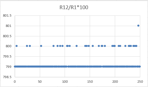
Figure 7-1 shows the test data of (R1+R2)/R1. You can see that the value fluctuation is ±0.13%.
 Figure 7-1 Tested (R1+R2)/R1 Under
25C
Figure 7-1 Tested (R1+R2)/R1 Under
25CFigure 7-2 shows the voltage output offset with different gain. All of them are below than 0.7 mV.
 Figure 7-2 Tested OPA1 Offset Under
25°C
Figure 7-2 Tested OPA1 Offset Under
25°CFigure 7-3 shows the test data of (R3+R4)/R3. You can see that the value fluctuation under GAIN32 is ±0.11%. For GAIN16, it is ±0.13%.
 Figure 7-3 Tested (R3+R4)/R3 Under
25°C
Figure 7-3 Tested (R3+R4)/R3 Under
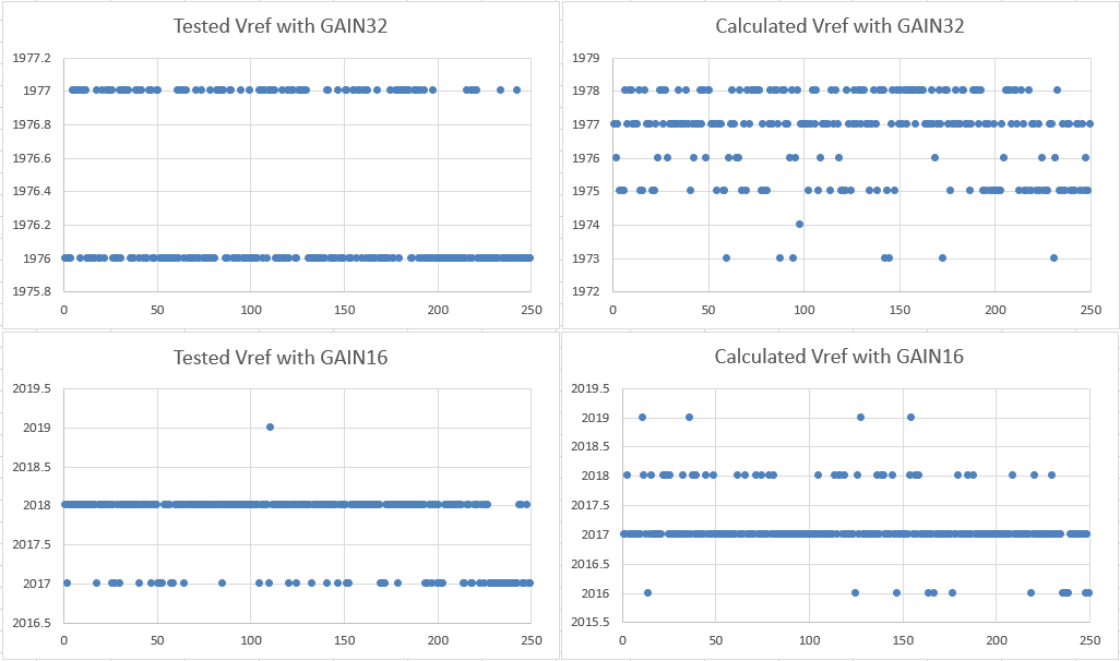
25°CTo evaluate the calibration accuracy, compare the calculated Vref through the Equation 2 and the tested Vref through ADC channel 13, when the current is 0. Pay attention that the tested data is the raw data from 12-Bit ADC with 1.4 V reference. The Vref is about 0.7 V, close to ½ ADC reference.
You can see that the tested Vref almost only have 1 or 2 ADC count change in two GAIN settings. If you treat the tested Vref as the accurate value for the GAIN32 setting, the max calculated Vref error is about 0.2%. For GAIN16 setting, it is about 0.15%.
As seen from these results, you can say that the self-calibration structure is very stable and has a very high accuracy.
 Figure 7-4 Tested and Calculated Vref
Under 25°C