SLAS975A November 2013 – August 2015 HD3SS6126
PRODUCTION DATA.
6 Specifications
6.1 Absolute Maximum Ratings
over operating free-air temperature range (unless otherwise noted)(1)| MIN | MAX | UNIT | ||
|---|---|---|---|---|
| Supply Voltage, VDD(2) | –0.3 | 4 | V | |
| Voltage | Differential I/O, High-bandwidth signal path: SSA0/1(p/n), SSB0/1(p/n), SSC0/1(p/n) | –0.5 | 4 | V |
| Differential I/O, Low-bandwidth signal path: HSAp/n), HSB(p/n), HSC(p/n) | -0.5 | 7 | ||
| Control pin and single ended I/O | –0.3 | VDD + 0.3 | ||
| Continuous power dissipation | See Thermal Information | |||
| Storage temperature, Tstg | –65 | 150 | °C | |
(1) Stresses beyond those listed under Absolute Maximum Ratings may cause permanent damage to the device. These are stress ratings only and functional operation of the device at these or any conditions beyond those indicated under Recommended Operating Conditions is not implied. Exposure to absolute-maximum-rated conditions for extended periods may affect device reliability.
(2) All voltage values, except differential voltages, are with respect to network ground terminal.
6.2 ESD Ratings
| VALUE | UNIT | |||
|---|---|---|---|---|
| V(ESD) | Electrostatic discharge | Human body model (HBM), per ANSI/ESDA/JEDEC JS-001(1) | ±2000 | V |
| Charged device model (CDM), per JEDEC specification JESD22-C101(2) | ±500 | |||
(1) JEDEC document JEP155 states that 500-V HBM allows safe manufacturing with a standard ESD control process.
(2) JEDEC document JEP157 states that 250-V CDM allows safe manufacturing with a standard ESD control process.
6.3 Recommended Operating Conditions
typical values for all parameters are at VCC = 3.3 V and TA = 25°C; all temperature limits are specified by design| MIN | NOM | MAX | UNIT | |||
|---|---|---|---|---|---|---|
| VDD | Supply voltage | 3.0 | 3.3 | 3.6 | V | |
| VIH | Input high voltage | Control Pins | 2.0 | VDD | V | |
| VIL | Input low voltage | Control Pins | –0.1 | 0.8 | V | |
| VI/O_Diff | Differential voltage | Switch I/O differential voltage for High-bandwidth signal path only: SSA0/1(p/n), SSB0/1(p/n), SSC0/1(p/n) | 0 | 1.8 | Vp-p | |
| VI/O_CM | Common voltage | Switch I/O common mode voltage for High-bandwidth signal path only: SSA0/1(p/n), SSB0/1(p/n), SSC0/1(p/n) | 0 | 2.0 | V | |
| TA | Operating free-air temperature | 0 | 70 | °C | ||
6.4 Thermal Information
| THERMAL METRIC | HD3SS6126 | UNIT | |
|---|---|---|---|
| RUA (WQFN) | |||
| 42 PINS | |||
| RθJA | Junction-to-ambient thermal resistance | 53.8 | °C/W |
| RθJC(top) | Junction-to-case (top) thermal resistance | 38.2 | °C/W |
| RθJB | Junction-to-board thermal resistance | 27.4 | °C/W |
| ψJT | Junction-to-top characterization parameter (1) | 5.6 | °C/W |
| ψJB | Junction-to-board characterization parameter (1) | 27.3 | °C/W |
(1) For more information about traditional and new thermal metrics, see Semiconductor and IC Package Thermal Metrics application report, SPRA953. Test conditions for ΨJB and ΨJT are clarified in the application report..
6.5 Electrical Characteristics – Device Parameters
over recommended operating conditions (unless otherwise noted)| PARAMETER | TEST CONDITIONS | MIN | TYP | MAX | UNIT | |
|---|---|---|---|---|---|---|
| ICC | Supply current | VDD = 3.6 V, SEL = VDD /GND; OE = GND; Outputs Floating | 2.4 | 3 | mA | |
| SEL | ||||||
| IIH | Input high current | VDD = 3.6 V, VIN = VDD | 95 | µA | ||
| IIL | Input high current | VDD = 3.6 V, VIN = GND | 1 | µA | ||
| HS_OE | ||||||
| IIH | Input high current | VDD = 3.6 V, VIN = VDD | 1 | µA | ||
| IIL | Input high current | VDD = 3.6 V, VIN = GND | 1 | µA | ||
| SSA0/1, SSB0/1, SSC0/1 | ||||||
| ILK | High-impedance leakage current | VDD = 3.6 V, VIN = 2 V, VOUT= 2 V, (ILK on open outputs Port B and C) |
130 | µA | ||
| VDD = 3.6 V, VIN = 2 V, VOUT= 2 V, (ILK on open outputs Port A) |
4 | |||||
| HSA, HSB, HSC | ||||||
| ILK | High-impedance leakage current | VDD = 3.6 V, VIN = 0 V, VOUT= 0 V to 4 V, HS_OE_IN = GND |
1 | µA | ||
6.6 Electrical Characteristics – Signal Switch Parameters
under recommended operating conditions; RL, RSC = 50 Ω, CL = 10 pF (unless otherwise noted)| PARAMETER | TEST CONDITIONS | MIN | TYP | MAX | UNIT | |
|---|---|---|---|---|---|---|
| SSA0/1(p/n), SSB0/1(p/n), SSC0/1(p/n) Signal Path | ||||||
| CON | Outputs ON capacitance | VIN = 0 V, outputs open, switch ON | 1.5 | pF | ||
| COFF | Outputs OFF capacitance | VIN = 0 V, outputs open, switch OFF | 1 | pF | ||
| RON | Output ON resistance | VDD = 3.3 V, VCM = 0 V – 2 V, IO = –8 mA |
5 | 8 | Ω | |
| ΔRON | ON resistance match between pairs of the same channel | VDD = 3.3 V; 0 V ≤ VIN ≤ 2 V; IO = –8 mA |
0.7 | Ω | ||
| RFLAT_ON | ON resistance flatness (RON(MAX)– RON(MIN) |
VDD = 3.3 V; –0 V ≤ VIN ≤ 2 V | 1.15 | Ω | ||
| RL | Differential return loss (VCM = 0 V) |
f = 0.3 MHz | –25 | dB | ||
| f = 2.5 GHz | –11 | |||||
| f = 4 GHz | –11 | |||||
| XTALK | Differential crosstalk (VCM = 0 V) |
f = 0.3 MHz | -85 | dB | ||
| f = 2.5 GHz | –35 | |||||
| f = 4 GHz | –33 | |||||
| OIRR | Differential off-isolation (VCM = 0 V) |
f = 0.3 MHz | -85 | dB | ||
| f = 2.5 GHz | -23 | |||||
| f = 4 GHz | –21 | |||||
| IL | Differential insertion loss (VCM = 0 V) |
f = 0.3 MHz | –0.43 | dB | ||
| f = 2.5 GHz | –1.1 | |||||
| f = 4 GHz | –1.3 | |||||
| BW | Bandwidth | At –3 dB | 10 | GHz | ||
| HSA(p/n), HSB(p/n), HSC(p/n) SIGNAL PATH | ||||||
| CON | Outputs ON capacitance | VIN = 0 V, Outputs Open, Switch ON | 6 | 7.5 | pF | |
| COFF | Outputs OFF capacitance | VIN = 0 V, Outputs Open, Switch OFF | 3.5 | 6 | pF | |
| RON | Output ON resistance | VDD = 3 V, VIN = 0 V, IO = 30 mA |
3 | 6 | Ω | |
| VDD = 3 V, VIN = 2.4 V, IO = 30 mA |
3.4 | 6 | ||||
| ΔRON | ON resistance match between pairs of the same channel | VDD = 3 V; VIN = 0 V; IO = 30 mA |
0.2 | Ω | ||
| VDD = 3 V; VIN = 1.7 V; IO = -15 mA |
0.2 | |||||
| RFLAT_ON | ON resistance flatness (RON(MAX)– RON(MIN ) |
VDD = 3 V; VIN = 0 V; IO = 30 mA |
1 | Ω | ||
| VDD = 3 V; VIN = 1.7 V; IO = –15 mA |
1 | |||||
| XTALK | Differential crosstalk (VCM = 0 V) | RL = 50 Ω, f = 250 MHz | –40 | dB | ||
| OIRR | Differential off-isolation (VCM = 0 V) | RL = 50 Ω, f = 250 MHz | –41 | dB | ||
| BW | Bandwidth | RL = 50 Ω | 0.9 | GHz | ||
(1) Specified by design
6.7 Switching Characteristics
over operating free-air temperature range (unless otherwise noted)| PARAMETER | TEST CONDITIONS | MIN | TYP | MAX | UNIT | |
|---|---|---|---|---|---|---|
| SSA0/1(p/n), SSB0/1(p/n), SSC0/1(p/n) Signal Path | ||||||
| ton | SEL-to-Switch ton | RSC and RL = 50 Ω, See Figure 1 | 70 | 250 | ns | |
| toff | SEL-to-Switch toff | RSC and RL = 50 Ω, See Figure 1 | 70 | 250 | ns | |
| tPD | Switch propagation delay | RSC and RL = 50 Ω, See Figure 3 | 85 | ps | ||
| tSK(O) | Interpair output skew (CH-CH) | RSC and RL = 50 Ω, See Figure 3 | 20 | ps | ||
| tSK(b-b) | Intrapair Output Skew (bit-bit) | RSC and RL = 50 Ω, See Figure 3 | 8 | ps | ||
| HSA(p/n), HSB(p/n), HSC(p/n) SIGNAL PATH | ||||||
| tON | SEL to Switch tON | See Figure 2 | 30 | ns | ||
| HS_OE to Switch tON | See Figure 2 | 17 | ||||
| tOFF | SEL to Switch tOFF | See Figure 2 | 12 | ns | ||
| HS_OE to Switch tOFF | See Figure 2 | 10 | ||||
| tPD(1) | Switch propagation delay | See Figure 3 | 250 | ps | ||
| tSK(O)(1) | Interpair output skew (CH-CH) | 100 | 200 | ps | ||
| tSK(P)(1) | Intrapair Output Skew (bit-bit) | 100 | 200 | ps | ||
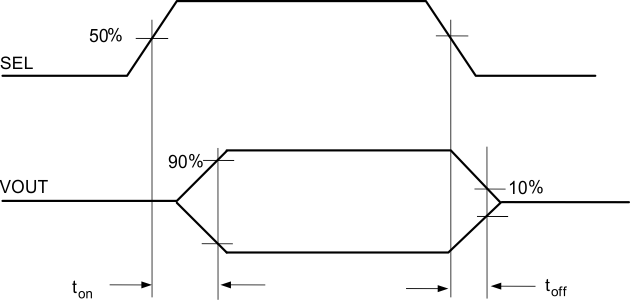 Figure 1. Select to Switch tON and tOFF
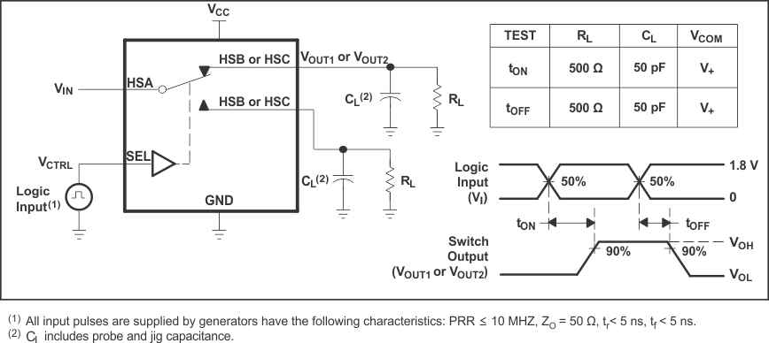 Figure 2. Turnon (tON) and Turnoff Time (tOFF)
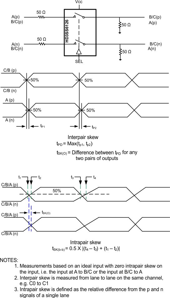 Figure 3. Propagation Delay and Skew
6.8 Typical Characteristics
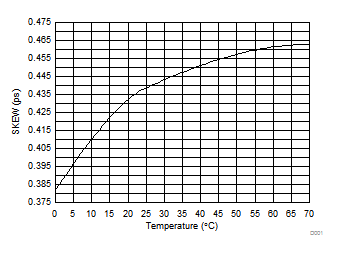 Figure 4. Intrapair Skew SSA to SSB Port
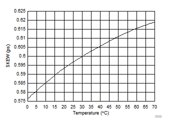 Figure 5. Intrapair Skew SSA to SSC Port