SLASEL1D June   2017  – August 2018 DAC60508 , DAC70508 , DAC80508

PRODUCTION DATA.  

  1. Features
  2. Applications
  3. Description
    1.     Device Images
      1.      Simplified Block Diagram
  4. Revision History
  5. Device Comparison Table
  6. Pin Configuration and Functions
    1.     Pin Functions
  7. Specifications
    1. 7.1 Absolute Maximum Ratings
    2. 7.2 ESD Ratings
    3. 7.3 Recommended Operating Conditions
    4. 7.4 Thermal Information
    5. 7.5 Electrical Characteristics
    6. 7.6 Typical Characteristics
  8. Detailed Description
    1. 8.1 Overview
    2. 8.2 Functional Block Diagram
    3. 8.3 Feature Description
      1. 8.3.1 Digital-to-Analog Converter (DAC) Architecture
        1. 8.3.1.1 DAC Transfer Function
        2. 8.3.1.2 Output Amplifiers
        3. 8.3.1.3 DAC Register Structure
          1. 8.3.1.3.1 DAC Register Synchronous and Asynchronous Updates
          2. 8.3.1.3.2 Broadcast DAC Register
          3. 8.3.1.3.3 CLEAR Operation (DACx0508C only)
      2. 8.3.2 Internal Reference
        1. 8.3.2.1 Reference Divider
        2. 8.3.2.2 Solder Heat Reflow
      3. 8.3.3 Device Reset Options
        1. 8.3.3.1 Power-on-Reset (POR)
        2. 8.3.3.2 Software Reset
    4. 8.4 Device Functional Modes
      1. 8.4.1 Stand-Alone Operation
      2. 8.4.2 Daisy-Chain Operation
      3. 8.4.3 Frame Error Checking
      4. 8.4.4 Power-Down Mode
    5. 8.5 Programming
    6. 8.6 Register Map
      1. 8.6.1 NOP Register (address = 0x00) [reset = 0x0000]
        1. Table 9. NOP Register Field Descriptions
      2. 8.6.2 DEVICE ID Register (address = 0x01) [reset = 0x---]
        1. Table 10. DEVICE ID Field Descriptions
      3. 8.6.3 SYNC Register (address = 0x2) [reset = 0xFF00]
        1. Table 11. SYNC Register Field Descriptions
      4. 8.6.4 CONFIG Register (address = 0x3) [reset = 0x0000]
        1. Table 12. CONFIG Register Field Descriptions
      5. 8.6.5 GAIN Register (address = 0x04) [reset = 0x---]
        1. Table 13. GAIN Register Field Descriptions
      6. 8.6.6 TRIGGER Register (address = 0x05) [reset = 0x0000]
        1. Table 14. TRIGGER Register Field Descriptions
      7. 8.6.7 BRDCAST Register (address = 0x6) [reset = 0x0000]
        1. Table 15. BRDCAST Register Field Descriptions
      8. 8.6.8 STATUS Register (address = 0x7) [reset = 0x0000]
        1. Table 16. STATUS Register Field Descriptions
      9. 8.6.9 DACx Register (address = 0x8 to 0xF) [reset = 0x0000 or 0x8000]
        1. Table 17. DACx Register Field Descriptions
  9. Application and Implementation
    1. 9.1 Application Information
      1. 9.1.1 Interfacing to Microcontroller
      2. 9.1.2 Programmable Current Source Circuit
    2. 9.2 Typical Application
      1. 9.2.1 Design Requirements
      2. 9.2.2 Detailed Design Procedure
      3. 9.2.3 Application Curve
  10. 10Power Supply Recommendations
  11. 11Layout
    1. 11.1 Layout Guidelines
    2. 11.2 Layout Examples
  12. 12Device and Documentation Support
    1. 12.1 Related Links
    2. 12.2 Receiving Notification of Documentation Updates
    3. 12.3 Community Resources
    4. 12.4 Trademarks
    5. 12.5 Electrostatic Discharge Caution
    6. 12.6 Glossary
  13. 13Mechanical, Packaging, and Orderable Information

Pin Configuration and Functions

RTE Package
16-Pin WQFN
Top View
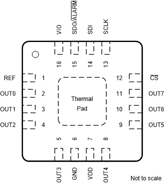
DAC80508 DAC70508 DAC60508 po_slasel1.gif
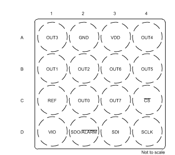
YZF Package
16-Pin DSBGA
Top View
DAC80508 DAC70508 DAC60508 YZF_po_slasel1.gif

Pin Functions

PIN TYPE DESCRIPTION
NAME WQFN NO. DSBGA NO.
REF 1 C1 I/O When using internal reference, this is the reference output voltage pin (default). When using an external reference, this is the reference input pin to the device.
OUT0 2 C2 O Analog output voltage from DAC 0.
OUT1 3 B1 O Analog output voltage from DAC 1.
OUT2 4 B2 O Analog output voltage from DAC 2.
OUT3 5 A1 O Analog output voltage from DAC 3.
GND 6 A2 GND Ground reference point for all circuitry on the device.
VDD 7 A3 PWR Analog supply voltage (2.7 V to 5.5 V).
OUT4 8 A4 O Analog output voltage from DAC 4.
OUT5 9 B4 O Analog output voltage from DAC 5.
OUT6 10 B3 O Analog output voltage from DAC 6.
OUT7 11 C3 O Analog output voltage from DAC 7.
CS 12 C4 I Active low serial data enable. This input is the frame synchronization signal for the serial data. When the signal goes low, it enables the serial interface input shift register.
SCLK 13 D4 I Serial interface clock.
SDI 14 D3 I Serial interface data input. Data are clocked into the input shift register on each falling edge of the SCLK pin.
SDO/ALARM 15 D2 O DACx0508. Serial interface data output (default). The SDO pin is in high impedance when CS pin is high. Data are clocked out of the input shift register on either rising or falling edges of the SCLK pin as specified by the FSDO bit. Alternatively the pin can be configured as an ALARM open-drain output to indicate a CRC or reference alarm event. If configured as ALARM a 10 kΩ, pull-up resistor to VIO is required.
CLR I DACx0508C. A low value on the CLR pin causes the DAC outputs of those channels configured for clear operation to update their registers and output to the reset value: zero scale (DACx0508Z) or midscale (DACx0508M). Bringing the CLR pin high causes the device to exit clear mode.
VIO 16 D1 PWR IO supply voltage (1.7 V to 5.5 V). This pin sets the I/O operating voltage for the serial interface.
Thermal Pad The thermal pad is located on the bottom-side of the WQFN package. The thermal pad should be connected to any internal PCB ground plane using multiple vias for good thermal performance.