SLDS216 December 2017 PGA302
PRODUCTION DATA.
- 1 Features
- 2 Applications
- 3 Description
- 4 Revision History
- 5 Description (continued)
- 6 Pin Configuration and Functions
-
7 Specifications
- 7.1 Absolute Maximum Ratings
- 7.2 ESD Ratings
- 7.3 Recommended Operating Conditions
- 7.4 Thermal Information
- 7.5 Overvoltage and Reverse Voltage Protection
- 7.6 Linear Regulators
- 7.7 Internal Reference
- 7.8 Internal Oscillator
- 7.9 Bridge Sensor Supply
- 7.10 Temperature Sensor Supply
- 7.11 Bridge Offset Cancel
- 7.12 P Gain and T Gain Input Amplifiers (Chopper Stabilized)
- 7.13 Analog-to-Digital Converter
- 7.14 Internal Temperature Sensor
- 7.15 Bridge Current Measurement
- 7.16 One Wire Interface
- 7.17 DAC Output
- 7.18 DAC Gain for DAC Output
- 7.19 Non-Volatile Memory
- 7.20 Diagnostics - PGA30x
- 7.21 Typical Characteristics
-
8 Detailed Description
- 8.1 Overview
- 8.2 Functional Block Diagram
- 8.3
Feature Description
- 8.3.1 Overvoltage and Reverse Voltage Protection
- 8.3.2 Linear Regulators
- 8.3.3 Internal Reference
- 8.3.4 Internal Oscillator
- 8.3.5 VBRGP and VBRGN Supply for Resistive Bridge
- 8.3.6 ITEMP Supply for Temperature Sensor
- 8.3.7 P Gain
- 8.3.8 T Gain
- 8.3.9 Bridge Offset Cancel
- 8.3.10 Analog-to-Digital Converter
- 8.3.11 Internal Temperature Sensor
- 8.3.12 Bridge Current Measurement
- 8.3.13 Digital Interface
- 8.3.14 OWI
- 8.3.15 I2C Interface
- 8.3.16 DAC Output
- 8.3.17 DAC Gain for DAC Output
- 8.3.18 Memory
- 8.3.19 Diagnostics
- 8.3.20 Digital Compensation and Filter
- 8.3.21 Revision ID
- 8.4 Device Functional Modes
- 8.5
Register Maps
- 8.5.1
Programmer's Model
- 8.5.1.1 Memory Map
- 8.5.1.2
Control and Status Registers
- 8.5.1.2.1 MICRO_INTERFACE_CONTROL (DI Page Address = 0x0) (DI Page Offset = 0x0C)
- 8.5.1.2.2 PSMON1 (M0 Address= 0x40000558) (DI Page Address = 0x2) (DI Page Offset = 0x58)
- 8.5.1.2.3 AFEDIAG (M0 Address= 0x4000055A) (DI Page Address = 0x2) (DI Page Offset = 0x5A)
- 8.5.1.2.4 P_GAIN_SELECT (DI Page Address = 0x2) (DI Page Offset = 0x47)
- 8.5.1.2.5 T_GAIN_SELECT (DI Page Address = 0x2) (DI Page Offset = 0x48)
- 8.5.1.2.6 TEMP_CTRL (DI Page Address = 0x2) (DI Page Offset = 0x4C)
- 8.5.1.2.7 OFFSET_CANCEL (DI Page Address = 0x2) (DI Page Offset = 0x4E)
- 8.5.1.2.8 PADC_DATA1 (DI Page Address = 0x0) (DI Page Offset = 0x10)
- 8.5.1.2.9 PADC_DATA2 (DI Page Address = 0x0) (DI Page Offset = 0x11)
- 8.5.1.2.10 TADC_DATA1 (DI Page Address = 0x0) (DI Page Offset = 0x14)
- 8.5.1.2.11 TADC_DATA2 (DI Page Address = 0x0) (DI Page Offset = 0x15)
- 8.5.1.2.12 DAC_REG0_1 (DI Page Address = 0x2) (DI Page Offset = 0x30)
- 8.5.1.2.13 DAC_REG0_2 (DI Page Address = 0x2) (DI Page Offset = 0x31)
- 8.5.1.2.14 OP_STAGE_CTRL (DI Page Address = 0x2) (DI Page Offset = 0x3B)
- 8.5.1.2.15 EEPROM_ARRAY (DI Page Address = 0x5) (DI Page Offset = 0x00 - 0x7F)
- 8.5.1.2.16 EEPROM_CACHE_BYTE0 (DI Page Address = 0x5) (DI Page Offset = 0x80)
- 8.5.1.2.17 EEPROM_CACHE_BYTE1 (DI Page Address = 0x5) (DI Page Offset = 0x81)
- 8.5.1.2.18 EEPROM_PAGE_ADDRESS (DI Page Address = 0x5) (DI Page Offset = 0x82)
- 8.5.1.2.19 EEPROM_CTRL (DI Page Address = 0x5) (DI Page Offset = 0x83)
- 8.5.1.2.20 EEPROM_CRC (DI Page Address = 0x5) (DI Page Offset = 0x84)
- 8.5.1.2.21 EEPROM_STATUS (DI Page Address = 0x5) (DI Page Offset = 0x85)
- 8.5.1.2.22 EEPROM_CRC_STATUS (DI Page Address = 0x5) (DI Page Offset = 0x86)
- 8.5.1.2.23 EEPROM_CRC_VALUE (DI Page Address = 0x5) (DI Page Offset = 0x87)
- 8.5.1.2.24 H0 (EEPROM Address= 0x40000000)
- 8.5.1.2.25 H1 (EEPROM Address= 0x40000002)
- 8.5.1.2.26 H2 (EEPROM Address= 0x40000004)
- 8.5.1.2.27 H3 (EEPROM Address= 0x40000006)
- 8.5.1.2.28 G0 (EEPROM Address= 0x40000008)
- 8.5.1.2.29 G1 (EEPROM Address= 0x4000000A)
- 8.5.1.2.30 G2 (EEPROM Address= 0x4000000C)
- 8.5.1.2.31 G3 (EEPROM Address= 0x4000000E)
- 8.5.1.2.32 N0 (EEPROM Address= 0x40000010)
- 8.5.1.2.33 N1 (EEPROM Address= 0x40000012)
- 8.5.1.2.34 N2 (EEPROM Address= 0x40000014)
- 8.5.1.2.35 N3 (EEPROM Address= 0x40000016)
- 8.5.1.2.36 M0 (EEPROM Address= 0x40000018)
- 8.5.1.2.37 M1 (EEPROM Address= 0x4000001A)
- 8.5.1.2.38 M2 (EEPROM Address= 0x4000001C)
- 8.5.1.2.39 M3 (EEPROM Address= 0x4000001E)
- 8.5.1.2.40 PADC_GAIN (EEPROM Address= 0x40000020)
- 8.5.1.2.41 TADC_GAIN (EEPROM Address= 0x40000021)
- 8.5.1.2.42 PADC_OFFSET (EEPROM Address= 0x40000022)
- 8.5.1.2.43 TADC_OFFSET (EEPROM Address= 0x40000024)
- 8.5.1.2.44 TEMP_SW_CTRL (EEPROM Address= 0x40000028)
- 8.5.1.2.45 DAC_FAULT_MSB (EEPROM Address= 0x4000002A)
- 8.5.1.2.46 LPF_A0_MSB (EEPROM Address= 0x4000002B)
- 8.5.1.2.47 LPF_A1 (EEPROM Address= 0x4000002C)
- 8.5.1.2.48 LPF_A2 (EEPROM Address= 0x4000002E)
- 8.5.1.2.49 .LPF_B1 (EEPROM Address= 0x40000030)
- 8.5.1.2.50 NORMAL_LOW (EEPROM Address= 0x40000032)
- 8.5.1.2.51 NORMAL_HIGH (EEPROM Address= 0x40000034)
- 8.5.1.2.52 LOW_CLAMP (EEPROM Address= 0x40000036)
- 8.5.1.2.53 HIGH_CLAMP (EEPROM Address= 0x40000038)
- 8.5.1.2.54 DIAG_BIT_EN (EEPROM Address= 0x4000003A)
- 8.5.1
Programmer's Model
- 9 Application and Implementation
- 10Power Supply Recommendations
- 11Layout
- 12Device and Documentation Support
- 13Mechanical, Packaging, and Orderable Information
8 Detailed Description
8.1 Overview
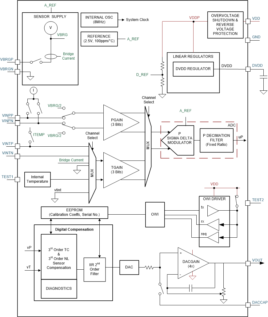
The PGA302 is a high accuracy, low drift, low noise, low power, and versatile signal conditioner automotive grade qualified device for resistive bridge pressure and temperature-sensing applications. The PGA302 accommodates various sensing element types, such as piezoresistive, ceramic film, and steel membrane. The typical applications supported are pressure sensor transmitter, transducer, liquid level meter, flow meter, strain gauge, weight scale, thermocouple, thermistor, 2-wire resistance thermometer (RTD), and resistive field transmitters. It can also be used in accelerometer and humidity sensor signal conditioning applications. The PGA302 provides bridge excitation voltages of 2.5 V. The PGA302 conditions sensing and temperature signals by amplification and digitization through the analog front end chain, and performs linearization and temperature compensation. The conditioned signals can be output in analog form. The signal data can also be accessed by an I2C digital interface and a GPIO port. The I2C interface can also be used to configure other function blocks inside the device. The PGA302 has the unique One-Wire Interface (OWI) that supports the communication and configuration through the power supply line. This feature allows to minimize the number of wires needed.
The PGA302 contains two separated analog-front end (AFE) chains for resistive bridge inputs and temperature-sensing inputs. Each AFE chain has its own gain amplifier. The resistive bridge input AFE chain consists of a programmable gain with 8 steps from 1.33 V/V to 200 V/V. For the temperature-sensing input AFE chain, the PGA302 provides a current source that can source up to 1000 µA for the optional external temperature sensing. This current source can also be used as a constant current bridge excitation. In addition, the PGA302 integrates an internal temperature sensor which can be configured as the input of the temperature-sensing AFE chain.
The digitalized signals after the ADC decimation filters are sent to the linearization and compensation calculation digital signal logic. A 128-byte EEPROM is integrated in the PGA302 to store sensor calibration coefficients and configuration settings as needed.
The PGA302 has a 14-bit DAC followed by a 4-V/V buffer gain stage. It supports industry standard ratiometric voltage output.
The diagnostic function monitors the operating conditions including power supplies overvoltage, undervoltage, or open AFE faults, DAC faults, and a DAC loopback option to check the integrity of the signal chains. The PGA302 also integrates an oscillator and power management. The PGA302 has a wide ambient temperature operating range from –40°C to +150°C. With a small package size, PGA302 has integrated all the functions needed for resistive bridge-sensing applications to minimize PCB area and simplify the overall application design.
8.2 Functional Block Diagram
8.3 Feature Description
In this section, individual functional blocks are described.
8.3.1 Overvoltage and Reverse Voltage Protection
The PGA302 includes overvoltage protection. This block protects the device from overvoltage conditions on the external power supply and shuts off device operation.
The PGA302 includes reverse voltage protection block. This block protects the device from reverse-battery conditions on the external power supply.
8.3.2 Linear Regulators
The PGA302 has DVDD regulator that provides the 1.8-V regulated voltage for the digital circuitry.
The Power-On Reset signal to the digital core is deasserted when DVDD are in regulation. Figure 9 shows the block diagram representation of the digital power-on-reset (POR) signal generation and Figure 10 shows the digital POR signal assertion and deassertion timing during VDD ramp up and ramp down. This timing shows that during power up, the digital core and the processor remains in reset state until DVDD is at stable levels.
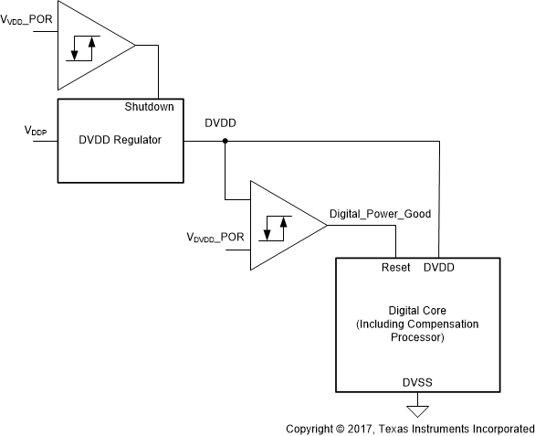 Figure 9. Digital Power-On-Reset Signal Generation
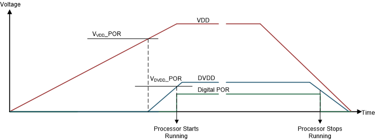 Figure 10. Digital Power-On-Reset Signal Generation
8.3.3 Internal Reference
PGA302 has internal bandgap reference.
The Reference is used to generate ADC reference voltage and Bridge drive voltage.
NOTE
The accurate reference is valid 50 µs after digital core starts running at power up.
8.3.4 Internal Oscillator
The device includes an internal 8-MHz oscillator. This oscillator provides the internal clock required for the various circuits in PGA302.
8.3.5 VBRGP and VBRGN Supply for Resistive Bridge
The Sensor Voltage Supply block of the PGA302 supplies power to the resistive bridge sensor. The sensor supply in the PGA302 is 2.5-V nominal output supply. This nominal supply is ratiometric to the precise internal Accurate Reference.
8.3.6 ITEMP Supply for Temperature Sensor
The ITEMP block in PGA302 supplies programmable current to an external temperature sensor such as PTC. The temperature sensor current source is ratiometric to the Reference.
The value of the current can be programmed using the ITEMP_CTRL bits in TEMP_CTRL register.
8.3.7 P Gain
The P Gain is designed with precision, low drift, low flicker noise, chopper-stabilized amplifiers. The P Gain is implemented as an Instrument Amplifier as shown in Figure 11.
The gain of this stage is adjustable using 3 bits in P_GAIN_SELECT register to accommodate sense elements with wide-range of signal spans.
The P Gain amplifier can be configured to measure half-bridge output. In this case, the half bridge can be connected to either VINPP or VINPN pins, while the other pin is internally connected to VBRG/2.
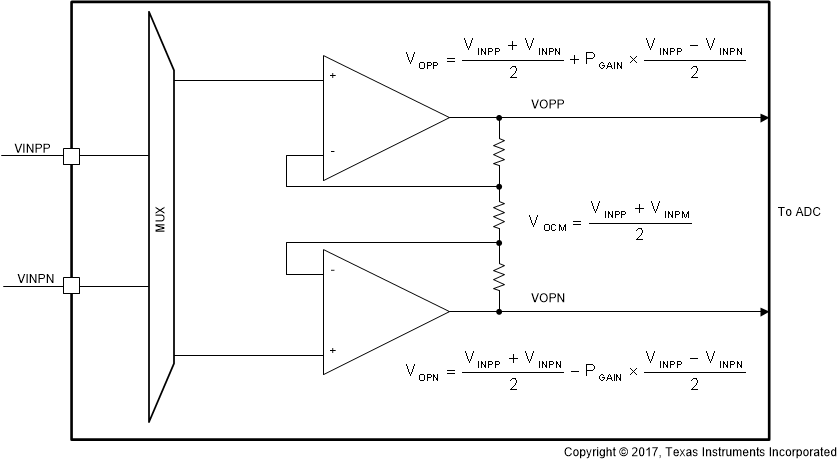 Figure 11. P Gain
8.3.8 T Gain
The T Gain is designed with precision, low drift, low flicker noise, chopper-stabilized amplifiers. The T Gain is identical in architecture to P Gain.
The gain of this stage is adjustable using 3 bits in T_GAIN_SELECT register to accommodate sense elements with wide-range of signal spans.
The T Gain amplifier can be configured to measure the following samples:
- VINTP-VINTN in Differential mode
- VINTP-GND in Single-ended mode
- Internal Temperature sensor voltage in Single-ended mode
- Bridge current in Single-ended mode
8.3.9 Bridge Offset Cancel
The PGA302 device implements a bridge offset cancel circuit at the input of the P GAIN in order to cancel large sensor bridge offsets. PGA302 achieves this by introducing a small current into one of the nodes of the bridge prior to the AFE gain. The selection of the offset is determined by the OFFSET_CANCEL register and the offset values are listed in Table 1.
Table 1. PGA302 Offset Cancel Implementation
| OFFSET_CANCEL Value | Applied Offset Voltage [mV] |
|---|---|
| 0x00 | 0 [OFF] |
| 0x01 | 3.65 |
| 0x02 | 7.3 |
| 0x03 | 10.95 |
| 0x04 | 14.6 |
| 0x05 | 18.28 |
| 0x06 | 21.9 |
| 0x07 | 25.55 |
| 0x08 | 29.2 |
| 0x09 | 32.85 |
| 0x0A | 36.5 |
| 0x0B | 40.15 |
| 0x0C | 43.8 |
| 0x0D | 47.45 |
| 0x0E | 51.1 |
| 0x0F | 54.75 |
Further the polarity of the applied offset can be changed by setting the OFFSET_CANCEL_SEL bit for positive offset or clearing the same bit for negative offset.
8.3.10 Analog-to-Digital Converter
The Analog-to-Digital Converter is for digitizing the P and T GAIN amplifier output. The digitized values are available in the respective channel ADC registers.
8.3.10.1 Sigma Delta Modulator for ADC
The sigma-delta modulator for ADC is a 4-MHz, second order, 3-bit quantizer sigma-delta modulator. The sigma-delta modulator can be halted using the ADC_CFG_1 register.
8.3.10.2 Decimation Filter for ADC
The decimation filter output rate can be configured for 96 µs, 128 µs, 192 µs or 256 µs.
The output of the decimation filter is 16-bit signed 2's complement value. Some example decimation output codes for given differential voltages at the input of the sigma delta modulator as shown in Table 2.
Table 2. Input Voltage to Output Counts for ADC
| SIGMA DELTA MODULATOR DIFFERENTIAL INPUT VOLTAGE | 16-BIT NOISE-FREE DECIMATOR OUTPUT |
|---|---|
| –2.5 V | –32768 (0x8000) |
| –-1.25 V | –16384 (0xC000) |
| 0 V | 0 (0x0000) |
| 1.25 V | 16383 (0x3FFF) |
| 2.5 V | 32767 (0x7FFF) |
8.3.10.3 Internal Temperature Sensor ADC Conversion
The nominal relationship between the device junction temperature and 16-bit TGAIN ADC Code for T GAIN = 4 V/V is shown in Equation 1
where
- TEMP is temperature in °C.
Table 3 shows ADC output for some example junction temperature values.
Table 3. Internal Temperature Sensor to ADC Value
| INTERNAL TEMPERATURE | 16-BIT ADC NOMINAL VALUE |
|---|---|
| –40°C | 4900 (0x1324) |
| 0°C | 5700 (0x1644) |
| 150°C | 8700 (0x21FC) |
8.3.10.4 ADC Scan Mode
The ADC is configured in auto scan mode, in which the ADC converts the pressure and temperature signals periodically.
8.3.10.4.1 P-T Multiplexer Timing in Auto Scan Mode
PGA302 has a multiplexer that multiplexes P and T channels into a single ADC. Figure 12 shows the multiplexing scheme.
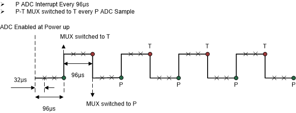 Figure 12. P-T multiplexing
8.3.11 Internal Temperature Sensor
PGA302 includes an internal temperature sensor whose voltage output is digitized by the ADC and made available to the processor. This digitized value is used to implement temperature compensation algorithms. Note that the voltage generated by the internal temperature sensor is proportional to the junction temperature.
Figure 13 shows the internal temperature sensor AFE.
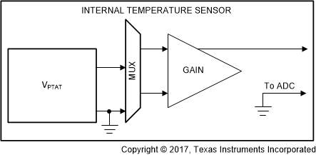 Figure 13. Temperature Sensor AFE
8.3.12 Bridge Current Measurement
PGA302 includes a bridge current measurement scheme. This digitized value can be used to implement temperature compensation algorithms. Note that the voltage generated is proportional to the bridge current.
Figure 14 shows the bridge current AFE.
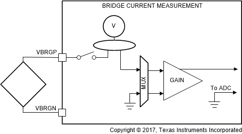 Figure 14. Bridge Current Measurement
8.3.13 Digital Interface
The digital interfaces are used to access (read and write) the internal memory spaces. The device has following modes of communication:
- One-wire interface (OWI)
The communication modes supported by PGA302 are referred to as digital interface in this document. For communication modes, PGA302 device operates as a slave device.
8.3.14 OWI
The device includes a OWI digital communication interface. The function of OWI is to enable writes to and reads from all memory locations inside PGA302 available for OWI access.
8.3.14.1 Overview of OWI Interface
The OWI digital communication is a master-slave communication link in which the PGA302 operates as a slave device only. The master device controls when data transmission begins and ends. The slave device does not transmit data back to the master until it is commanded to do so by the master.
The VDD pin of PGA302 is used as OWI interface, so that when PGA302 is embedded inside of a system module, only two pins are needed (VDD and GND) for communication. The OWI master communicates with PGA302 by modulating the voltage on VDD pin while PGA302 communicates with the master by modulating current on VDD pin. The PGA302 processor has the ability to control the activation and deactivation of the OWI interface based upon the OWI Activation pulse driven on VDD pin.
Figure 15 shows a functional equivalent circuit for the structure of the OWI circuitry.
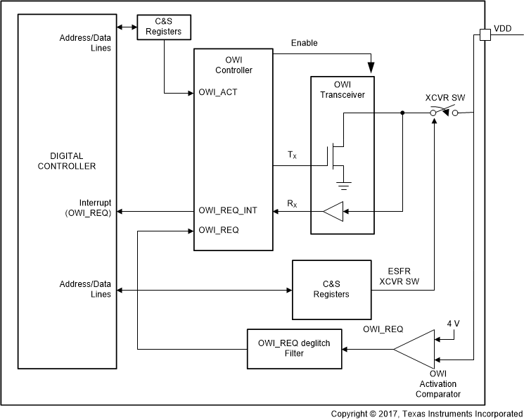 Figure 15. OWI System Components
8.3.14.2 Activating and Deactivating the OWI Interface
8.3.14.2.1 Activating OWI Communication
The OWI master initiates OWI communication by generating OWI Activation Pulse on VDD pin. When PGA302 receives a valid OWI Activation pulse, it prepares itself for OWI communication.
To activate OWI communication, the OWI master must Generate an OWI Activation pulse on VDD pin. Figure 16 illustrates the OWI Activation Pulse that is generated by the Master.
 Figure 16. OWI Activation Using Overvoltage Drive
8.3.14.2.2 Deactivating OWI Communication
To deactivate OWI communication and restart the processor inside PGA302 (if it was in reset), the following step must be performed by the OWI Master
- The processor reset should be deasserted by writing 0 to MICRO_RESET bit in
MICRO_INTERFCE_CONTROL register and access to Digital Interface should be disabled by writing 0 to IF_SEL bit in the MICRO_INTERFACE_CONTROL register.
8.3.14.3 OWI Protocol
8.3.14.3.1 OWI Frame Structure
8.3.14.3.1.1 Standard field structure:
Data is transmitted on the one-wire interface in byte sized packets. The first bit of the OWI field is the start bit. The next 8 bits of the field are data bits to be processed by the OWI control logic. The final bit in the OWI field is the stop bit. A group of fields make up a transmission frame. A transmission frame is composed of the fields necessary to complete one transmission operation on the one-wire interface. The standard field structure for a one-wire field is shown in Figure 17
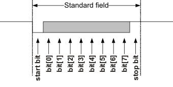 Figure 17. Standard OWI Field
8.3.14.3.1.2 Frame Structure
A complete one-wire data transmission operation is done in a frame with the structure is shown in Figure 18.
 Figure 18. OWI Transmission Frame, N = 1 to 8
Each transmission frame must have a Synchronization field and command field followed by zero to a maximum of 8 data fields. The sync field and command fields are always transmitted by the master device. The data field(s) may be transmitted either by the master or the slave depending on the command given in the command field. It is the command field which determines direction of travel of the data fields (master-to-slave or slave-to-master). The number of data fields transmitted is also determined by the command in the command field. The inter-field wait time is optional and may be necessary for the slave or the master to process data that has been received.
If OWI remains idle in either logic 0 or logic 1 state, for more than 15 ms, then the PGA302 communication will reset and will expect to receive a sync field as the next data transmission from the master.
8.3.14.3.1.3 Sync Field
The Sync field is the first field in every frame that is transmitted by the master. The Sync field is used by the slave device to compute the bit width transmitted by the master. This bit width will be used to accurately receive all subsequent fields transmitted by the master. The format of the Sync field is shown in Figure 19.
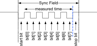 Figure 19. The OWI Sync Field.
NOTE
Consecutive SYNC field bits are measured and compared to determine if a valid SYNC field is being transmitted to the PGA302 is valid. If the difference in bit widths of any two consecutive SYNC field bits is greater than +/- 25%, then PGA302 will ignore the rest of the OWI frame (that is, the PGA302 will not respond to the OWI message).
8.3.14.3.1.4 Command Field
The command field is the second field in every frame sent by the master. The command field contains instructions about what to do with and where to send the data that is transmitted to the slave. The command field can also instruct the slave to send data back to the master during a Read operation. The number of data fields to be transmitted is also determined by the command in the command field. The format of the command field is shown in Figure 20.
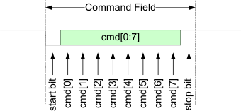 Figure 20. The OWI Command Field.
8.3.14.3.1.5 Data Field(s)
After the Master has transmitted the command field in the transmission frame, Zero or more Data Fields are transmitted to the slave (Write operation) or to the master (Read operation). The Data fields can be raw EEPROM data or address locations in which to store data. The format of the data is determined by the command in the command field. The typical format of a data field is shown in Figure 21.
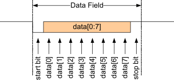 Figure 21. The OWI Data Field.
8.3.14.3.2 OWI Commands
The following is the list of five OWI commands supported by PGA302:
- OWI Write
- OWI Read Initialization
- OWI Read Response
- OWI Burst Write of EEPROM Cache
- OWI Burst Read from EEPROM Cache
8.3.14.3.2.1 OWI Write Command
| Field Location | Description | Bit 7 | Bit 6 | Bit 5 | Bit 4 | Bit 3 | Bit 2 | Bit 1 | Bit 0 |
|---|---|---|---|---|---|---|---|---|---|
| Command Field | Basic Write Command | 0 | P2 | P1 | P0 | 0 | 0 | 0 | 1 |
| Data Field 1 | Destination Address | A7 | A6 | A5 | A4 | A3 | A2 | A1 | A0 |
| Data Field 2 | Data byte to be written | D7 | D6 | D5 | D4 | D3 | D2 | D1 | D0 |
The P2, P1, P0 bits in the command field determine the memory page that is being accessed by the OWI. The memory page decode is shown in Table 4.
Table 4. OWI Memory Page Decode
| P2 | P1 | P0 | Memory Page |
|---|---|---|---|
| 0 | 0 | 0 | Control and Status Registers, DI_PAGE_ADDRESS = 0x00 |
| 0 | 1 | 0 | Control and Status Registers, DI_PAGE_ADDRESS = 0x02 |
| 1 | 0 | 1 | EEPROM Cache/Cells |
| 1 | 1 | 0 | Reserved |
| 1 | 1 | 1 | Control and Status Registers, DI_PAGE_ADDRESS = 0x07 |
8.3.14.3.2.2 OWI Read Initialization Command
| Field Location | Description | Bit 7 | Bit 6 | Bit 5 | Bit 4 | Bit 3 | Bit 2 | Bit 1 | Bit 0 |
|---|---|---|---|---|---|---|---|---|---|
| Command Field | Read Init Command | 0 | P2 | P1 | P0 | 0 | 0 | 1 | 0 |
| Data Field 1 | Fetch Address | A7 | A6 | A5 | A4 | A3 | A2 | A1 | A0 |
The P2, P1, P0 bits in the command field determine the memory page that is being accessed by the OWI. The memory page decode is shown in Table 4.
8.3.14.3.2.3 OWI Read Response Command
| Field Location | Description | Bit 7 | Bit 6 | Bit 5 | Bit 4 | Bit 3 | Bit 2 | Bit 1 | Bit 0 |
|---|---|---|---|---|---|---|---|---|---|
| Command Field | Read Response Command | 0 | 1 | 1 | 1 | 0 | 0 | 1 | 1 |
| Data Field 1 | Data Retrieved (OWI drives data out) | D7 | D6 | D5 | D4 | D3 | D2 | D1 | D0 |
The P2, P1, P0 bits in the command field determine the memory page that is being accessed by the OWI. The memory page decode is shown in Table 4.
8.3.14.3.2.4 OWI Burst Write Command (EEPROM Cache Access)
| Field Location | Description | Bit 7 | Bit 6 | Bit 5 | Bit 4 | Bit 3 | Bit 2 | Bit 1 | Bit 0 |
|---|---|---|---|---|---|---|---|---|---|
| Command Field | EE_CACHE Write Command Cache Bytes (0–7) | 1 | 1 | 0 | 1 | 0 | 0 | 0 | 0 |
| Data Field 1 | 1st Data Byte to be written | D7 | D6 | D5 | D4 | D3 | D2 | D1 | D0 |
| Data Field 2 | 2nd Data Byte to be written | D7 | D6 | D5 | D4 | D3 | D2 | D1 | D0 |
8.3.14.3.2.5 OWI Burst Read Command (EEPROM Cache Access)
| Field Location | Description | Bit 7 | Bit 6 | Bit 5 | Bit 4 | Bit 3 | Bit 2 | Bit 1 | Bit 0 |
|---|---|---|---|---|---|---|---|---|---|
| Command Field | Burst read Response (8-bytes) | 1 | 1 | 0 | 1 | 0 | 0 | 1 | 1 |
| Data Field 1 | 1st Data Byte Retrieved EE Cache Byte 0 |
D7 | D6 | D5 | D4 | D3 | D2 | D1 | D0 |
| Data Field 2 | 2nd Data Byte Retrieved EE Cache Byte 1 |
D7 | D6 | D5 | D4 | D3 | D2 | D1 | D0 |
8.3.14.3.3 OWI Operations
8.3.14.3.3.1 Write Operation
The write operation on the one-wire interface is fairly straightforward. The command field specifies the write operation, where the subsequent data bytes are to be stored in the slave, and how many data fields are going to be sent. Additional command instructions can be sent in the first few data fields if necessary. The write operation is illustrated in Figure 22.
 Figure 22. Write Operation, N = 1 to 8.
8.3.14.3.3.2 Read Operation
The read operation requires two consecutive transmission frames to move data from the slave to the master. The first frame is the Read Initialization Frame. It tells the slave to retrieve data from a particular location within the slave device and prepare to send it over the OWI. The data location may be specified in the command field or may require additional data fields for complete data location specification. The data will not be sent until the master commands it to be sent in the subsequent frame called the Read Response Frame. During the read response frame the data direction changes from master → slave to slave → master right after the read response command field is sent. Enough time exist between the command field and data field in order to allow the signal drivers time to change direction. This wait time is 20 µs and the timer for this wait time is located on the slave device. After this wait time is complete the slave will transmit the requested data. The master device is expected to have switched its signal drivers and is ready to receive data. The Read frames are shown in Figure 23.
 Figure 23. Read Initialization Frame, N = 1 to 8.
 Figure 24. Read Response Frame, N = 1 to 8
8.3.14.3.3.3 EEPROM Burst Write
The EEPORM burst write is used to write 2 bytes of data to the EEPROM Cache using one OWI frame. This allows fast programming of EEPROM in the manufacturing line. Note that the EEPROM page has to be selected before transferring the contents of the EEPROM memory cells to the EEPROM cache.
8.3.14.3.3.4 EEPROM Burst Read
The EEPORM burst read is used to read 2 bytes of data from the EEPROM Cache using one OWI frame. The Burst Read command is used for fast read the EEPROM cache contents in the manufacturing line. The read process is used to verify the writes to the EEPROM cache.
8.3.14.4 OWI Communication Error Status
PGA302 detects errors in OWI communication. OWI_ERROR_STATUS_LO and OWI_ERROR_STATUS_HI registers contain OWI communication error bits. The communication errors detected include:
- Out of range communication baud rate
- Invalid SYNC field
- Invalid STOP bits in command and data
- Invalid OWI command
8.3.15 I2C Interface
The device includes an Inter-Integrated Circuit (I2C) digital communication interface. The main function of the I2C is to enable writes to, and reads from, all addresses available for I2C access.
8.3.15.1 Overview of I2C Interface
I2C is a synchronous serial communication standard that requires the following two pins for communication:
- SDA: I2C Serial Data Line (SDA)
- SCL: I2C Serial Clock Line (SCL)
I2C communicates in a master/slave style communication bus where one device, the master, can initiate data transmission. The device always acts as the slave device in I2C communication, where the external device that is communicating to it acts as the master node. The master device is responsible for initiating communication over the SDA line and supplying the clock signal on the SCL line. When the I2C SDA line is pulled low it is considered a logical zero, and when the I2C SDA line is floating high it is considered a logical one. For the I2C interface to have access to memory locations other than test register space, the IF_SEL bit in the Micro/Interface Control Test register (MICRO_IF_SEL_T) has to be set to logic one.
8.3.15.2 I2C Interface Protocol
The basic Protocol of the I2C frame for a Write operation is shown in Figure 25:
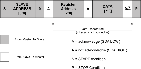 Figure 25. I2C Write Operation: A Master-Transmitter Addressing a PGA302 Slave With a 7-Bit Slave Address
The diagram represents the data fed into or out from the I2C SDA port.
The basic data transfer is to send 2 bytes of data to the specified Slave Address. The first data field is the register address and the second data field is the data sent or received.
The I2C Slave Address is used to determine which memory page is being referenced. Table 5 shows the mapping of the slave address to the memory page.
Table 5. Slave Addresses
| Slave Address | PGA302 Memory Page |
|---|---|
| 0x40 | Test Registers |
| 0x42 | Control and Status Registers, DI_PAGE_ADDRESS = 0x02 |
| 0x45 | EEPROM Cache/Cells |
| 0x46 | Reserved |
| 0x47 | Control and Status Registers, DI_PAGE_ADDRESS = 0x07 |
The basic PGA302 I2C Protocol for a read operation is shown in Figure 26.
 Figure 26. I2C Read Operation: A Master-Transmitter Addressing a PGA302 Slave With a 7-Bit Slave Address
The Slave Address determines the memory page. The R/W bit is set to 0.
The Register Address specifies the 8-bit address of the requested data.
The Repeat Start Condition replaces the write data from the above write operation description. This informs the PGA302 devices that Read operation will take place instead of a write operation.
The second Slave Address contains the memory page from which the data will be retrieved. The R/W bit is set to 1.
Slave data is transmitted after the acknowledge is received by the master.
Table 6 lists a few examples of I2C Transfers.
Table 6. I2C Transfers Examples
| Command | Master to Slave Data on I2C SDA |
|---|---|
| Read COM_MCU_TO_DIF_B0 |
Slave Address: 100 0000 Register Address: 0000 0100 |
| Write 0x80 to Control and Status Registers 0x30 (DAC_REG0_1) |
Slave Address: 100 0010 Register Address: 0011 0000 Data: 1000 0000 |
| Read from EEPROM Byte 7 |
Slave Address: 100 0101 Register Address: 0000 0111 |
8.3.15.3 Clocking Details of I2C Interface
The device samples the data on the SDA line when the rising edge of the SCL line is high, and is changed when the SCL line is low. The only exceptions to this indication are start, stop, or repeated start conditions as shown in Figure 27.
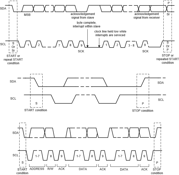 Figure 27. I2C Clocking Details
8.3.16 DAC Output
The device includes a 14-bit digital to analog converter that produces ratiometric output voltage with respect to the VDD supply. The DAC can be disabled by writing 0 to DAC_ENABLE bit in DAC_CTRL_STATUS register.
When the processor undergoes a reset, the DAC registers are driven to 0x000 code.
8.3.17 DAC Gain for DAC Output
The DAC Gain buffer is a buffer stage for the DAC Output. The final stage of DAC Gain is connected to Vddp and Ground. This gives the ability to drive VOUT voltage close to VDD voltage.
8.3.17.1 Connecting DAC Output to DAC GAIN Input
The DAC output can either be connected to TEST1 test pin or can connected to DAC GAIN input as shown in Figure 28. Note that DAC output can be connected to DAC GAIN input by setting TEMP_MUX_DAC_EN bit in AMUX_CTRL register to 1.
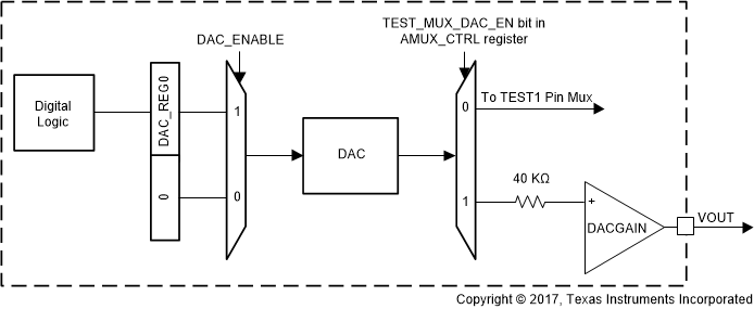 Figure 28. Connecting DAC to DAC GAIN
8.3.18 Memory
8.3.18.1 EEPROM Memory
Figure 29 shows the EEPROM structure. The contents of each EEPROM must be transferred to the EEPROM Cache before writes (that is, the EEPROM can be programmed 2 bytes at a time). The EEPROM reads occur without the EEPROM cache.
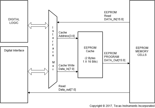 Figure 29. Structure of EEPROM Interface
8.3.18.1.1 EEPROM Cache
The EEPROM Cache serves as temporary storage of data being transferred to selected EEPROM locations during the programming process.
8.3.18.1.2 EEPROM Programming Procedure
For programming the EEPROM, the EEPROM is organized in 64 pages of 2 bytes each. The EEPROM memory cells are programmed by writing to the 2-byte EEPROM Cache. The contents of the cache are transferred to EEPROM memory cells by selecting the EEPROM memory page.
- Select the EEPROM page by writing the upper 6 bits of the 7-bit EEPROM address to EEPROM_PAGE_ADDRESS register
- Load the 2-byte EEPROM Cache by writing to the EEPROM_CACHE registers.
- User can erase by writing 1 to the ERASE bit in EEPROM_CTRL register and 1 to the PROGAM bit in the EEPROM_CTRL register simultaneously.
8.3.18.1.3 EEPROM Programming Current
The EEPROM programming process will result in an additional 1.5-mA current on the VDD pin for the duration of programming.
8.3.18.1.4 CRC
The last byte of the EEPROM memory is reserved for the CRC. This CRC value covers all data in the EEPROM memory. Every time the last byte is programmed, the CRC value is automatically calculated and validated. The validation process checks the calculated CRC value with the last byte programmed in the EEPROM memory cell. If the calculated CRC matches the value programmed in the last byte, the CRC_GOOD bit is set in EEPROM_CRC_STATUS register.
The CRC check can also be initiated at any time by setting the CALCULATE_CRC bit in the EEPROM_CRC register. The status of the CRC calculation is available in CRC_CHECK_IN_PROG bit in EEPROM_CRC_STATUS register, while the result of the CRC validation is available in CRC_GOOD bit in EEPROM_CRC_STATUS register.
The CRC calculation pseudo code is as follows:
currentCRC8 = 0xFF; // Current value of CRC8

for NextData

D = NextData;

C = currentCRC8;

  begin

      nextCRC8_BIT0 = D_BIT7 ^ D_BIT6 ^ D_BIT0 ^ C_BIT0 ^ C_BIT6 ^ C_BIT7;

      nextCRC8_BIT1 = D_BIT6 ^ D_BIT1 ^ D_BIT0 ^ C_BIT0 ^ C_BIT1 ^ C_BIT6;

      nextCRC8_BIT2 = D_BIT6 ^ D_BIT2 ^ D_BIT1 ^ D_BIT0 ^ C_BIT0 ^ C_BIT1 ^ C_BIT2 ^ C_BIT6;

      nextCRC8_BIT3 = D_BIT7 ^ D_BIT3 ^ D_BIT2 ^ D_BIT1 ^ C_BIT1 ^ C_BIT2 ^ C_BIT3 ^ C_BIT7;

      nextCRC8_BIT4 = D_BIT4 ^ D_BIT3 ^ D_BIT2 ^ C_BIT2 ^ C_BIT3 ^ C_BIT4;

      nextCRC8_BIT5 = D_BIT5 ^ D_BIT4 ^ D_BIT3 ^ C_BIT3 ^ C_BIT4 ^ C_BIT5;

      nextCRC8_BIT6 = D_BIT6 ^ D_BIT5 ^ D_BIT4 ^ C_BIT4 ^ C_BIT5 ^ C_BIT6;

      nextCRC8_BIT7 = D_BIT7 ^ D_BIT6 ^ D_BIT5 ^ C_BIT5 ^ C_BIT6 ^ C_BIT7;

   end

   currentCRC8 = nextCRC8_D8;

endfor
NOTE
The EEPROM CRC calculation is complete 340 µs after digital core starts running at power up.
8.3.19 Diagnostics
This section describes the diagnostics.
8.3.19.1 Power Supply Diagnostics
The device includes modules to monitor the power supply for faults. The internal power rails that are monitored are:
- VDD Voltage, thresholds are generated using High Voltage Reference
- DVDD Voltage, thresholds are generated using High Voltage Reference
- Bridge Supply Voltage, thresholds are generated using High Voltage Reference
- Internal Oscillator Supply Voltage, thresholds are generated using High Voltage Reference
- Reference Output Voltage, thresholds are generated using High Voltage Reference
The electrical specifications lists the voltage thresholds for each of power rails.
8.3.19.2 Sensor Connectivity/Gain Input Faults
The device includes circuits to monitor bridge connectivity and temperature sensor connectivity fault. Note that temperature sensor connectivity fault is monitored only in 16-pin package option. Specifically, the device monitors the bridge pins for opens (including loss of connection from the sensor), short-to-ground, and short-to-sensor supply.
Table 7. Sensor Connectivity/Gain Input Faults (Diagnostic Resistors Active)
| Fault No. | Fault Mode | Chip Behavior |
|---|---|---|
| 1 | VBRGP Open | VINP_UV and PGAIN_UV flags set |
| 2 | VBRGN Open | N/A |
| 3 | VINPP Open | VINP_UV and PGAIN_UV flags set |
| 4 | VINPN Open | VINP_UV and PGAIN_UV flags set |
| 5 | VBRGP Shorted to VBRGN | VBRG_UV, VINP_UV and PGAIN_UV flags set |
| 6 | VBRGP Shorted to VINPP | VINP_OV and PGAIN_OV flags set |
| 7 | VBRGP Shorted to VINPN | VINP_OV and PGAIN_OV flags set |
| 8 | VINPP shorted to VINPN | N/A |
| 9 | VINNPP shorted to VBRGN | VINP_UV and PGAIN_UV flags set |
| 10 | Temperature path is differential, VINTP Open | TGAIN_UV flag set |
| 11 | Temperature path is differential, VINTN Open | VINT_OV and TGAIN_OV flags set |
| 12 | Temperature path is differential, VINTP shorted to VINTN | N/A |
| 13 | Temperature path is single-ended, VINTP Open | TGAIN_UV flag set |
| 14 | Temperature path is single-ended, VINTN Shorted to ground | TGAIN_UV flag set |
The thresholds for connectivity fault are derived off of VBRDG voltage.
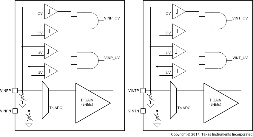 Figure 30. Block Diagram of Bridge Connectivity Diagnostics
8.3.19.3 Gain Output Diagnostics
The device includes modules that verify that the output signal of each gain is within a certain range. This ensures that gain stages in the signal chain are working correctly. AVDD voltage is used to generate the thresholds voltages for comparison.
When a fault is detected, the corresponding bit in AFEDIAG register is set. Even after the faulty condition is removed, the fault bits will remain latched. To remove the fault, M0 software should read the fault bit and write a logic zero back to the bit. A system reset will clear the fault.
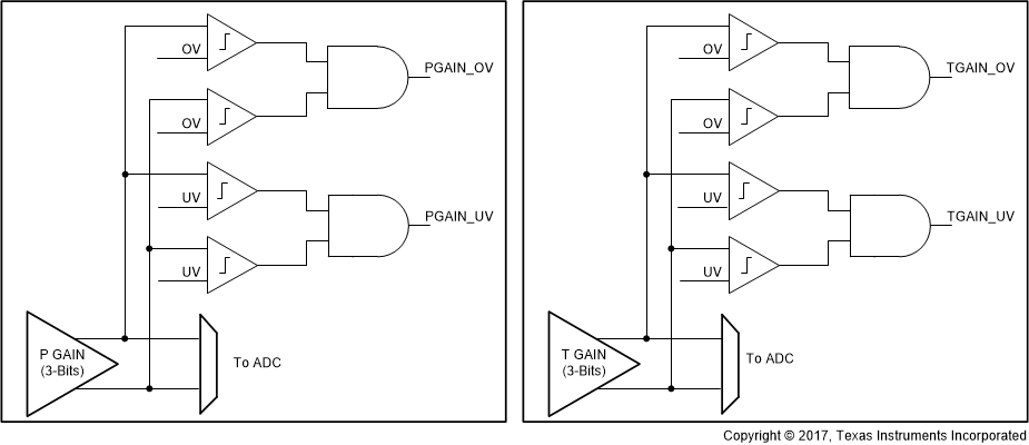 Figure 31. Block Diagram of Gain Output Diagnostics
8.3.19.4 PGA302 Harness Open Wire Diagnostics
PGA302 allows for Open Wire Diagnostics to be performed in the ECU. Specifically, the ECU can detect open VDD or Open GND wire by installing a pullup or pulldown on VOUT line.
Table 8. PGA302 Harness Faults
| Fault No. | Device VDD | Device GND | Device VOUT | Remark | Device status after removal of failure |
|---|---|---|---|---|---|
| 1 | 5 V | 0 V | Pullup to VDD | Normal Connection with VOUT to Pulled to VDD | Resumes normal operation |
| 2 | 5 V | 0 V | Pulldown to GND | Normal Connection with VOUT to Pulled to GND | Device Reset |
| 3 | 20 V | 0 V | GND to VDD | Overvoltage | Device Reset |
| 4 | Open | 0 V | Pullup to VDD = 5 V | Open VDD with VOUT Pulled to VDD | Device Reset |
| 5 | Open | 0 V | Pulldown to GND | Open VDD with VOUT Pulled to GND | Device Reset |
| 6 | 5 V | Open | Pullup to VDD = 5 V | Open GND with VOUT Pulled to VDD | Device Reset |
| 7 | 5 V | Open | Pulldown to GND | Open GND with VOUT Pulled to GND | Device Reset |
| 8 | 0 V | 20 V | Pullup to VDD | Reverse Voltage with VOUT Pulled to VDD | Device Reset |
| 9 | 0 V | 20 V | Pulldown to GND | Reverse Voltage with VOUT Puledl to GND | Physical Damage possible. |
| 10 | 0 V | 0 V | Pullup to VDD | VDD Shorted to GND with VOUT Pulled to VDD | Device Reset |
| 11 | 0 V | 0 V | Pulldown to GND | VDD Shorted to GND with VOUT Pulled to GND | Device Reset |
| 12 | 20 V | 20 V | Pullup to VDD | GND Shorted to VDD with VOUT Pulled to VDD | Device Reset. Physical Damage possible. |
| 13 | 20 V | 20 V | Pulldown to GND | GND Shorted to VDD with VOUT Pulled to GND | Device Reset |
| 14 | 20 V | 0 V | 20 V | VOUT Shorted to VDD | Device Reset. Physical Damage possible. |
| 15 | 20 V | 0 V | 0 V | VOUT Shorted to GND | Resumes normal operation |
Figure 32 shows the possible harness open wire faults on VDD and GND pins.
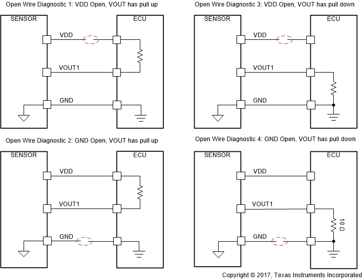 Figure 32. Harness Open Wire Diagnostics
Table 9 summarizes the open wire diagnostics and the corresponding resistor pull values that allows the ECU to detect open harness faults.
Table 9. Typical Internal Pulldown Settings
| Open Harness | ECU Pull Direction | Max Pull Value (KΩ) | State of PGA302 during fault condition | ECU Voltage Level (VOUT/OWI pin) |
|---|---|---|---|---|
| VDD | Pullup | 50 | PGA302 is off. Leakage currents present (especially at high temp) | VDD – (Ileak1 × Rpullup) |
| GND | Pullup | N/A | PGA302 is off, all power rails pulled up to VDD | VDD |
| VDD | Pulldown | N/A | PGA302 is off, all power rails pulled down to ground | GND |
| GND | Pulldown | 50 | PGA302 is off, leakage current pushed into VOUT pin (thru the chip's ground). | GND + (Ileak2 × Rpulldown) |
8.3.19.5 EEPROM CRC and TRIM Error
The last Byte in the EEPROM stores the CRC for all the data in EEPROM.
The user can verify the EEPROM CRC at any time. When the last byte is programmed into the EEPROM, the device automatically calculates the CRC and updates the CRC_GOOD bit in EEPROM CRC Status Register. The validity of the CRC can also be verified by initiating the CRC check by setting the control bit CACULATE_CRC bit in EEPROM_CRC register.
The device also has analog trim values. The validity of the analog trim values is checked on power up. The validity of the trim values can be inferred using the CRC_GOOD bit in the TRIM_CRC_STATUS register.
8.3.20 Digital Compensation and Filter
PGA300 implements a second order TC and NL correction of the pressure input. The corrected output is then filtered using a second order IIR filter and then written to the output register.
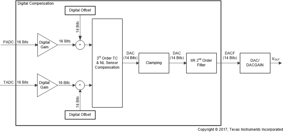 Figure 33. Digital Compensation Equation
8.3.20.1 Digital Gain and Offset
The digital compensation implements digital gain and offset shown in Equation 2 and Equation 3:
where
- a0 is the digital gain
- and b0 is the digital offset for PADC
where
- a1 is the digital gain
- and b1 is the digital offset for TADC.
8.3.20.2 TC and NL Correction
The compensation is shown in Equation 4:
8.3.20.3 Clamping
The output of the compensation is clamped. The low and high clamp values are programmable.
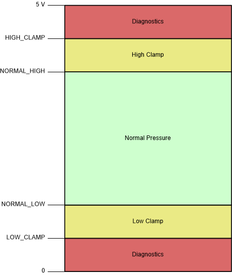 Figure 34. PGA302 Clamping of Output
8.3.20.4 Filter
The IIR filter is shown in Equation 5 and Equation 6:
8.3.21 Revision ID
PGA302 includes Revision ID registers. These registers are read-only and represent the device revision and is not unique for every device in a certain revision.
8.4 Device Functional Modes
There are two functional modes in the PGA302: A Running mode of operation where the digital processing logic is enabled and the Reset mode where the digital processing logic is in reset.
In the Running mode, the I2C and OWI digital interfaces are not allowed to access the PGA302 device memory space. The only communication with the device can be established by accessing the COMBUF communication buffer registers.
The Reset mode is generally used for PGA302 device configuration. In this mode, the I2C or OWI interfaces are allowed to read and write to the device memory. In this mode, the digital processing logic is in reset which means that no device internal signal processing is performed therefore no output data is being generated from the device itself.
8.5 Register Maps
8.5.1 Programmer's Model
8.5.1.1 Memory Map
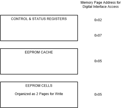 Figure 35. Memory Map
8.5.1.2 Control and Status Registers
Table 10. PGA302 Control and Status Registers
| Register Name | DI Page Address | DI Offset Address | EEPROM Address | R/W | D7 | D6 | D5 | D4 | D3 | D2 | D1 | D0 |
|---|---|---|---|---|---|---|---|---|---|---|---|---|
| H0_LSB | N/A | N/A | 0x40000000 | RW | H0 [7:0] | |||||||
| H0_MSB | N/A | N/A | 0x40000001 | RW | H0 [15:8] | |||||||
| H1_LSB | N/A | N/A | 0x40000002 | RW | H1 [7:0] | |||||||
| H1_MSB | N/A | N/A | 0x40000003 | RW | H1 [15:8] | |||||||
| H2_LSB | N/A | N/A | 0x40000004 | RW | H2 [7:0] | |||||||
| H2_MSB | N/A | N/A | 0x40000005 | RW | H2 [15:8] | |||||||
| H3_LSB | N/A | N/A | 0x40000006 | RW | H3 [7:0] | |||||||
| H3_MSB | N/A | N/A | 0x40000007 | RW | H3 [15:8] | |||||||
| G0_LSB | N/A | N/A | 0x40000008 | RW | G0 [7:0] | |||||||
| G0_MSB | N/A | N/A | 0x40000009 | RW | G0 [15:8] | |||||||
| G1_LSB | N/A | N/A | 0x4000000A | RW | G1 [7:0] | |||||||
| G1_MSB | N/A | N/A | 0x4000000B | RW | G1 [15:8] | |||||||
| G2_LSB | N/A | N/A | 0x4000000C | RW | G2 [7:0] | |||||||
| G2_MSB | N/A | N/A | 0x4000000D | RW | G2 [15:8] | |||||||
| G3_LSB | N/A | N/A | 0x4000003E | RW | G3 [7:0] | |||||||
| G3_MSB | N/A | N/A | 0x4000003F | RW | G3 [15:8] | |||||||
| N0_LSB | N/A | N/A | 0x40000010 | RW | N0 [7:0] | |||||||
| N0_MSB | N/A | N/A | 0x40000011 | RW | N0 [15:8] | |||||||
| N1_LSB | N/A | N/A | 0x40000012 | RW | N1 [7:0] | |||||||
| N1_MSB | N/A | N/A | 0x40000013 | RW | N1 [15:8] | |||||||
| N2_LSB | N/A | N/A | 0x40000014 | RW | N2 [7:0] | |||||||
| N2_MSB | N/A | N/A | 0x40000015 | RW | N2 [15:8] | |||||||
| N3_LSB | N/A | N/A | 0x40000016 | RW | N3 [7:0] | |||||||
| N3_MSB | N/A | N/A | 0x40000017 | RW | N3 [15:8] | |||||||
| M0_LSB | N/A | N/A | 0x40000018 | RW | M0 [7:0] | |||||||
| M0_MSB | N/A | N/A | 0x40000019 | RW | M0 [15:8] | |||||||
| M1_MSB | N/A | N/A | 0x4000001A | RW | M1 [7:0] | |||||||
| M1_LSB | N/A | N/A | 0x4000001B | RW | M1 [15:8] | |||||||
| M2_LSB | N/A | N/A | 0x4000001C | RW | M2 [7:0] | |||||||
| M2_MSB | N/A | N/A | 0x4000001D | RW | M2 [15:8] | |||||||
| M3_LSB | N/A | N/A | 0x4000001E | RW | M3 [7:0] | |||||||
| M3_MSB | N/A | N/A | 0x4000001F | RW | M3 [15:8] | |||||||
| PADC_GAIN | N/A | N/A | 0x40000020 | RW | PADC_GAIN [7:0] | |||||||
| TADC_GAIN | N/A | N/A | 0x40000021 | RW | TADC_GAIN [7:0] | |||||||
| PADC_OFFSET_BYTE0 | N/A | N/A | 0x40000022 | RW | PADC_OFFSET [7:0] | |||||||
| PADC_OFFSET_BYTE1 | N/A | N/A | 0x40000023 | RW | PADC_OFFSET [15:8] | |||||||
| TADC_OFFSET_BYTE0 | N/A | N/A | 0x40000024 | RW | TADC_OFFSET [7:0] | |||||||
| TADC_OFFSET_BYTE1 | N/A | N/A | 0x40000025 | RW | TADC_OFFSET [15:8] | |||||||
| P_GAIN_ SELECT |
0x2 | 0x47 | 0x40000026 | RW | P_INV | P_MUX_ CTRL[1] |
P_MUX_ CTRL[0] |
PSEM | P_GAIN[2] | P_GAIN[1] | P_GAIN[0] | |
| T_GAIN_ SELECT |
0x2 | 0x48 | 0x40000027 | RW | T_INV | Write 0 | T_MUX_ CTRL[1] |
T_MUX_ CTRL[0] |
TSEM | T_GAIN[2] | T_GAIN[1] | T_GAIN[0] |
| TEMP_CTRL | 0x2 | 0x4C | N/A | RW | Write 0 | ITEMP_ CTRL[2] |
ITEMP_ CTRL[1] |
ITEMP_ CTRL[0] |
||||
| TEMP_SW_CTRL | N/A | N/A | 0x40000028 | RW | Write 0 | ITEMP_ CTRL[2] |
ITEMP_ CTRL[1] |
ITEMP_ CTRL[0] |
OFFSET_EN | DIAG_ENABLE | DACCAP_EN | EEPROM_LOCK |
| OFFSET_CANCEL | 0x2 | 0x4E | 0x40000029 | RW | Write 0 | OFFSET_ CANCEL_VAL[4] |
OFFSET CANCEL_VAL[3] |
OFFSET CANCEL_VAL[2] |
OFFSET CANCEL_VAL[1] |
OFFSET CANCEL_VAL[0] |
||
| DAC_FAULT_MSB | N/A | N/A | 0x4000002A | RW | DAC_FAULT[15:8] | |||||||
| LPF_A0_MSB | N/A | N/A | 0x4000002B | RW | A0 [15:8] | |||||||
| LPF_A1_LSB | N/A | N/A | 0x4000002C | RW | A1 [7:0] | |||||||
| LPF_A1_MSB | N/A | N/A | 0x4000002D | RW | A1 [15:8] | |||||||
| LPF_A2_LSB | N/A | N/A | 0x4000002E | RW | A2 [7:0] | |||||||
| LPF_A2_MSB | N/A | N/A | 0x4000002F | RW | A2 [15:8] | |||||||
| LPF_B1_LSB | N/A | N/A | 0x40000030 | RW | B1 [7:0] | |||||||
| LPF_B1_MSB | N/A | N/A | 0x40000031 | RW | B1 [15:8] | |||||||
| PADC_DATA1 | 0x2 | 0x20 | N/A | R | PADC_DATA [7:0] | |||||||
| PADC_DATA2 | 0x2 | 0x21 | N/A | R | PADC_DATA [15:8] | |||||||
| TADC_DATA1 | 0x2 | 0x24 | N/A | R | TADC_DATA [7:0] | |||||||
| TADC_DATA2 | 0x2 | 0x25 | N/A | R | TADC_DATA [15:8] | |||||||
| DAC_REG0_1 | 0x2 | 0x30 | N/A | RW | DAC_VALUE [7:0] | |||||||
| DAC_REG0_2 | 0x2 | 0x31 | N/A | RW | DAC_VALUE [11:8] | |||||||
| OP_STAGE_CTRL | 0x2 | 0x3B | N/A | RW | DACCAP_EN | |||||||
| NORMAL_LOW_LSB | N/A | N/A | 0x40000032 | RW | NORMAL_DAC_LOW [7:0] | |||||||
| NORMAL_LOW_MSB | N/A | N/A | 0x40000033 | RW | NORMAL_DAC_LOW [11:8] | |||||||
| NORMAL_HIGH_LSB | N/A | N/A | 0x40000034 | RW | NORMAL_DAC_HIGH [7:0] | |||||||
| NORMAL_HIGH_MSB | N/A | N/A | 0x40000035 | RW | NORMAL_DAC_HIGH [11:8] | |||||||
| LOW_CLAMP_LSB | N/A | N/A | 0x40000036 | RW | CLAMP_DAC_LOW [7:0] | |||||||
| LOW_CLAMP_MSB | N/A | N/A | 0x40000037 | RW | CLAMP_DAC_LOW [11:8] | |||||||
| HIGH_CLAMP_LSB | N/A | N/A | 0x40000038 | RW | CLAMP_DAC_HIGH [7:0] | |||||||
| HIGH_CLAMP_MSB | N/A | N/A | 0x40000039 | RW | CLAMP_DAC_HIGH [11:8] | |||||||
| DIAG_BIT_EN | N/A | N/A | 0x4000003A | RW | TGAIN_UV_EN | TGAIN_OV_EN | PGAIN_UV_EN | PGAIN_OV_EN | VINT_OV_EN | VINP_UV_EN | VINP_OV_EN | |
| PSMON1 | 0x2 | 0x58 | N/A | RW | DVDD_OV | REF_UV | REF_OV | VBRG_UV | VBRG_OV | |||
| AFEDIAG | 0x2 | 0x5A | N/A | RW | TGAIN_UV | TGAIN_OV | PGAIN_UV | PGAIN_OV | VINT_OV | VINP_UV | VINP_OV | |
| SERIAL_NUMBER_BYTE0 | N/A | N/A | 0x4000003B | RW | SERIAL_NUMBER [7:0] | |||||||
| SERIAL_NUMBER_BYTE1 | N/A | N/A | 0x4000003C | RW | SERIAL_NUMBER [15:8] | |||||||
| SERIAL_NUMBER_BYTE2 | N/A | N/A | 0x4000003D | RW | SERIAL_NUMBER [23:16] | |||||||
| SERIAL_NUMBER_BYTE3 | N/A | N/A | 0x4000003E | RW | SERIAL_NUMBER [31:24] | |||||||
| USER_FREE_SPACE | N/A | N/A | 0x4000003F- 0x4000007E |
RW | ||||||||
| EEPROM_CRC | N/A | N/A | 0x4000007F | RW | EEPROM_CRC [7:0] | |||||||
| MICRO_ INTERFACE_ CONTROL |
0x0 | 0x0C | N/A | RW | MICRO_RESET | IF_SEL | ||||||
| EEPROM ARRAY | 0x5 | 0x00-0x7F | N/A | R | ||||||||
| EEPROM_CACHE | 0x5 | 0x80-0x81 | N/A | RW | ||||||||
| EEPROM_PAGE_ ADDRESS |
0x5 | 0x82 | N/A | RW | ADDR[5] | ADDR[4] | ADDR[3] | ADDR[2] | ADDR[1] | ADDR[0] | ||
| EEPROM_CTRL | 0x5 | 0x83 | N/A | RW | Write 0 | ERASE | PROGRAM | |||||
| EEPROM_CRC | 0x5 | 0x84 | N/A | RW | CALCULATE _CRC |
|||||||
| EEPROM_STATUS | 0x5 | 0x85 | N/A | R | PROGRAM_IN _PROGRESS |
ERASE_IN _PROGRESS |
READ_IN _PROGRESS |
|||||
| EEPROM_CRC _STATUS |
0x5 | 0x86 | N/A | R | CRC_GOOD | CRC_CHECK _IN_PROG |
||||||
| EEPROM_CRC _VALUE |
0x5 | 0x87 | N/A | R | EEPROM_CRC_VALUE [7:0] | |||||||
8.5.1.2.1 MICRO_INTERFACE_CONTROL (DI Page Address = 0x0) (DI Page Offset = 0x0C)
| 7 | 6 | 5 | 4 | 3 | 2 | 1 | 0 |
| Reserved | Reserved | Reserved | Reserved | Reserved | Reserved | MICRO_RESET | IF_SEL |
| N/A | N/A | N/A | N/A | N/A | N/A | R/W-0 | R/W-0 |
Table 11. MICRO_INTERFACE_CONTROL Register Field Descriptions
| Bit | Field | Type | Reset | Description |
|---|---|---|---|---|
| 0 | IF_SEL | R/W | 0x00 | 1: Digital Interface accesses the memory 0: Ccontroller accesses the memory |
| 1 | MICRO_RESET | R/W | 0x00 | 1: Controller Reset 0: Controller Running |
| 2:7 | Reserved | N/A | 0x00 | Reserved |
8.5.1.2.2 PSMON1 (M0 Address= 0x40000558) (DI Page Address = 0x2) (DI Page Offset = 0x58)
| 7 | 6 | 5 | 4 | 3 | 2 | 1 | 0 |
| Reserved | Reserved | Reserved | DVDD_OV | REF_UV | REF_OV | VBRG_UV | VBRG_OV |
| N/A | R/W-0 | N/A | R/W-0 | R/W-0 | R/W-0 | R/W-0 | R/W-0 |
Table 12. PSMON1 Register Field Descriptions
| Bit | Field | Type | Reset | Description |
|---|---|---|---|---|
| 0 | VBRG_OV | R/W | 0x00 | Read:
1: VBRG is overvoltage 0: VBRG is not overvoltage Write: 1: Clears VBRG_OV bit 0: No Action |
| 1 | VBRG_UV | R/W | 0x00 | Read:
1: VBRG is undervoltage 0: VBRG is not undervoltage Write: 1: Clears VBRG_UV bit 0: No Action |
| 2 | REF_OV | R/W | 0x00 | Read:
1: Reference is overvoltage 0: Reference is not overvoltage Write: 1: Clears REF_OV bit 0: No Action |
| 3 | REF_UV | R/W | 0x00 | Read:
1: Reference is undervoltage 0: Reference is not undervoltage Write: 1: Clears REF_UV bit 0: No Action |
| 4 | DVDD_OV | R/W | 0x00 | Read:
1: DVDD is overvoltage 0: DVDD is not overvoltage Write: 1: Clears DVDD_OV bit 0: No Action |
| 5 | Reserved | N/A | 0x00 | Reserved |
| 6 | Reserved | N/A | 0x00 | Reserved |
| 7 | Reserved | N/A | 0x00 | Reserved |
8.5.1.2.3 AFEDIAG (M0 Address= 0x4000055A) (DI Page Address = 0x2) (DI Page Offset = 0x5A)
| 7 | 6 | 5 | 4 | 3 | 2 | 1 | 0 |
| TGAIN_UV | TGAIN_OV | PGAIN_UV | PGAIN_OV | Reserved | VINT_OV | VINP_UV | VINP_OV |
| R/W-0 | R/W-0 | R/W-0 | R/W-0 | R/W-0 | R/W-0 | R/W-0 | R/W-0 |
Table 13. AFEDIAG Register Field Descriptions
| Bit | Field | Type | Reset | Description |
|---|---|---|---|---|
| 0 | VINP_OV | R/W | 0x00 | Read:
1: Indicates overvoltage at input pins of P Gain 0: Indicates no overvoltage at input pins of P Gain Write: 1: Clears VINP_OV bit 0: No Action |
| 1 | VINP_UV | R/W | 0x00 | Read:
1: Indicates undervoltage at input pins of P Gain 0: Indicates no undervoltage at input pins of P Gain Write: 1: Clears VINP_UV bit 0: No Action |
| 2 | VINT_OV | R/W | 0x00 | Read:
1: Indicates overvoltage at input pins of T Gain 0: Indicates no overvoltage at input pins of T Gain Write: 1: Clears VINT_OV bit 0: No Action |
| 3 | Reserved | R/W | 0x00 | |
| 4 | PGAIN_OV | R/W | 0x00 | Read:
1: Indicates overvoltage at output of P Gain 0: Indicates no overvoltage at output of P Gain Write: 1: Clears PGAIN_OV bit 0: No Action |
| 5 | PGAIN_UV | R/W | 0x00 | Read:
1: Indicates undervoltage at output of P Gain 0: Indicates no undervoltage at output of P Gain Write: 1: Clears PGAIN_UV bit 0: No Action |
| 6 | TGAIN_OV | R/W | 0x00 | Read:
1: Indicates overvoltage at output of T Gain 0: Indicates no overvoltage at output of T Gain Write: 1: Clears TGAIN_OV bit 0: No Action |
| 7 | TGAIN_UV | R/W | 0x00 | Read:
1: Indicates ubdervoltage at output of T Gain 0: Indicates no undervoltage at output of T Gain Write: 1: Clears TGAIN_UV bit 0: No Action |
8.5.1.2.4 P_GAIN_SELECT (DI Page Address = 0x2) (DI Page Offset = 0x47)
| 7 | 6 | 5 | 4 | 3 | 2 | 1 | 0 |
| P_INV | Reserved | P_MUX_ CTRL[1] |
P_MUX_ CTRL[0] |
PSEM | P_GAIN[2] | P_GAIN[1] | P_GAIN[0] |
| R/W-0 | R/W-0 | R/W-0 | R/W-0 | R/W-0 | R/W-0 | R/W-0 | R/W-0 |
Table 14. P_GAIN_SELECT Register Field Descriptions
| Bit | Field | Type | Reset | Description |
|---|---|---|---|---|
| 0 | P_GAIN[0] | R/W | 0x00 | See Electrical Parameters for Gain Selections |
| 1 | P_GAIN[1] | R/W | 0x00 | |
| 2 | P_GAIN[2] | R/W | 0x00 | |
| 3 | PSEM | R/W | 0x00 | 1: Differential mode 0: Single-ended mode |
| 4 | P_MUX_CTRL[0] | R/W | 0x00 | P Channel Input MUX: 00: VINPP - VINPN 01: VINPP - 1.25V 10: 1.25V - VINPN When P_INV =1 the order is reversed |
| 5 | P_MUX_CTRL[1] | R/W | 0x00 | |
| 6 | Reserved | R/W | 0x00 | Reserved |
| 7 | P_INV | R/W | 0x00 | 1: Inverts the output of the GAIN Output for pressure channel 0: No Inversion |
8.5.1.2.5 T_GAIN_SELECT (DI Page Address = 0x2) (DI Page Offset = 0x48)
| 7 | 6 | 5 | 4 | 3 | 2 | 1 | 0 |
| T_INV | T_MUX_ CTRL[2] |
T_MUX_ CTRL[1] |
T_MUX_ CTRL[0] |
TSEM | T_GAIN[2] | T_GAIN[1] | T_GAIN[0] |
| R/W-0 | R/W-0 | R/W-0 | R/W-0 | R/W-0 | R/W-0 | R/W-0 | R/W-0 |
Table 15. T_GAIN_SELECT Register Field Descriptions
| Bit | Field | Type | Reset | Description |
|---|---|---|---|---|
| 0 | T_GAIN[0] | R/W | 0x00 | See Electrical Parameters for Gain Selections |
| 1 | T_GAIN[1] | R/W | 0x00 | |
| 2 | T_GAIN[2] | R/W | 0x00 | |
| 3 | TSEM | R/W | 0x00 | 1: Differential mode 0: Single-ended mode |
| 4 | T_MUX_CTRL[0] | R/W | 0x00 | 0b000: External Temperature Sensor 0b001: TEST1 0b010: Internal Temperature Sensor 0b011: Bridge Current 0b100: ITEMP Pin Voltage |
| 5 | T_MUX_CTRL[1] | R/W | 0x00 | |
| 6 | T_MUX_CTRL[2] | R/W | 0x00 | |
| 7 | T_INV | R/W | 0x00 | 1: Inverts the output of the GAIN Output for pressure channel 0: No Inversion |
8.5.1.2.6 TEMP_CTRL (DI Page Address = 0x2) (DI Page Offset = 0x4C)
| 7 | 6 | 5 | 4 | 3 | 2 | 1 | 0 |
| ITEMP_DST_SEL | ITEMP_ CTRL[2] |
ITEMP_ CTRL[1] |
ITEMP_ CTRL[0] |
Reserved | Reserved | Reserved | Reserved |
| R/W-0 | R/W-1 | R/W-0 | R/W-0 | N/A | N/A | N/A | N/A |
Table 16. TEMP_CTRL Register Field Descriptions
| Bit | Field | Type | Reset | Description |
|---|---|---|---|---|
| 0:3 | Reserved | N/A | 0x00 | Reserved |
| 4:6 | ITEMP_CTRL[3:0] | R/W | 0x00 | 0x00: 50 µA 0x01: 100 µA 0x02: 200 µA 0x03: 1000 µA 0x04 - 0x07: OFF |
| 7 | ITEMP_DST_SEL | R/W | 0x00 | 0: ITEMP is driven to VINTP pin 1: ITEMP is driven to ITEMP pin |
8.5.1.2.7 OFFSET_CANCEL (DI Page Address = 0x2) (DI Page Offset = 0x4E)
| 7 | 6 | 5 | 4 | 3 | 2 | 1 | 0 |
| Reserved | Reserved | Reserved | OFFSET_ CANCEL_SEL |
OFFSET CANCEL_VAL[3] |
OFFSET CANCEL_VAL[2] |
OFFSET CANCEL_VAL[1] |
OFFSET CANCEL_VAL[0] |
| N/A | N/A | N/A | R/W-0 | R/W-0 | R/W-0 | R/W-0 | R/W-0 |
Table 17. OFFSET_CANCEL Register Field Descriptions
| Bit | Field | Type | Reset | Description |
|---|---|---|---|---|
| 0 | OFFSET_CANCEL_VAL[0] | R/W | 0x00 | 0x00: 0 mV 0x01: 3.65 mV 0x02: 7.3 mV 0x03: 10.95 mV 0x04: 14.6 mV 0x05: 18.28 mV 0x06: 21.9 mV 0x07: 25.55 mV 0x08: 29.2mV 0x09: 32.85 mV 0x0A: 36.5 mV 0x0B: 40.15mV 0x0C: 43.8 mV 0x0D: 47.45mV 0x0E: 51.1 mV 0x0F: 54.75 mV |
| 1 | OFFSET_CANCEL_VAL[1] | R/W | 0x00 | |
| 2 | OFFSET_CANCEL_VAL[2] | R/W | 0x00 | |
| 3 | OFFSET_CANCEL_VAL[3] | R/W | 0x00 | |
| 4 | OFFSET_CANCEL_SEL | R/W | 0x00 | 1: Offset current is connected to VINPP pin (Positive Offset) 0: Offset current is connected to VINPN pin (Negative Offset) |
| 5:7 | Reserved | N/A | 0x00 | Reserved |
8.5.1.2.8 PADC_DATA1 (DI Page Address = 0x0) (DI Page Offset = 0x10)
- To read PADC_DATA from Digital Interface, the least significant byte/word should be read first. This returns the least significant byte/word. The most significant bytes are latched into a shadow register. Reads to the Digital Interface addresses 0x11 return data from this shadow register.
- In 16-bit mode, PADC_DATA1 will be the least significant byte and PADC_DATA2 is the most significant byte.
| 7 | 6 | 5 | 4 | 3 | 2 | 1 | 0 |
| PADC_DATA [7:0] | |||||||
| R-0 | R-0 | R-0 | R-0 | R-0 | R-0 | R-0 | R-0 |
Table 18. PADC_DATA1 Register Field Descriptions
| Bit | Field | Type | Reset | Description |
|---|---|---|---|---|
| 0:7 | PADC_DATA [7:0] | R | 0x00 | Pressure ADC Output LS Byte |
8.5.1.2.9 PADC_DATA2 (DI Page Address = 0x0) (DI Page Offset = 0x11)
- To read PADC_DATA from Digital Interface, the least significant byte/word should be read first. This returns the least significant byte/word. The most significant bytes are latched into a shadow register. Reads to the Digital Interface addresses 0x11 return data from this shadow register.
- In 16-bit mode, PADC_DATA1 will be the least significant byte and PADC_DATA2 is the most significant byte.
| 7 | 6 | 5 | 4 | 3 | 2 | 1 | 0 |
| PADC_DATA [15:8] | |||||||
| R-0 | R-0 | R-0 | R-0 | R-0 | R-0 | R-0 | R-0 |
Table 19. PADC_DATA2 Register Field Descriptions
| Bit | Field | Type | Reset | Description |
|---|---|---|---|---|
| 0:7 | PADC_DATA | R | 0x00 | Pressure ADC Output MS Byte |
8.5.1.2.10 TADC_DATA1 (DI Page Address = 0x0) (DI Page Offset = 0x14)
- To read TADC_DATA from Digital Interface, the least significant byte/word should be read first. This returns the least significant byte/word. The most significant bytes are latched into a shadow register. Reads to the Digital Interface addresses 0x15 return data from this shadow register.
- In 16-bit mode, TADC_DATA1 will be the least significant byte and TADC_DATA2 is the most significant byte.
| 7 | 6 | 5 | 4 | 3 | 2 | 1 | 0 |
| TADC_DATA [7:0] | |||||||
| R-0 | R-0 | R-0 | R-0 | R-0 | R-0 | R-0 | R-0 |
Table 20. TADC_DATA1 Register Field Descriptions
| Bit | Field | Type | Reset | Description |
|---|---|---|---|---|
| 0:7 | TADC_DATA | R | 0x00 | Temperature ADC Output LS Byte |
8.5.1.2.11 TADC_DATA2 (DI Page Address = 0x0) (DI Page Offset = 0x15)
- To read TADC_DATA from Digital Interface, the least significant byte/word should be read first. This returns the least significant byte/word. The most significant bytes are latched into a shadow register. Reads to the Digital Interface addresses 0x15 return data from this shadow register.
- In 16-bit mode, TADC_DATA1 will be the least significant byte and TADC_DATA2 is the most significant byte.
| 7 | 6 | 5 | 4 | 3 | 2 | 1 | 0 |
| TADC_DATA [15:8] | |||||||
| R-0 | R-0 | R-0 | R-0 | R-0 | R-0 | R-0 | R-0 |
Table 21. TADC_DATA2 Register Field Descriptions
| Bit | Field | Type | Reset | Description |
|---|---|---|---|---|
| 0:7 | TADC_DATA | R | 0x00 | Temperature ADC Output MS Byte |
8.5.1.2.12 DAC_REG0_1 (DI Page Address = 0x2) (DI Page Offset = 0x30)
DAC Register Usage:
| 7 | 6 | 5 | 4 | 3 | 2 | 1 | 0 |
| DAC_VAL [7:0] | |||||||
| R/W-0 | R/W-0 | R/W-0 | R/W-0 | R/W-0 | R/W-0 | R/W-0 | R/W-0 |
Table 22. DAC_REG0_1 Register Field Descriptions
| Bit | Field | Type | Reset | Description |
|---|---|---|---|---|
| 0:7 | DAC_VAL | R/W | 0x00 | DAC Output value LS Byte |
8.5.1.2.13 DAC_REG0_2 (DI Page Address = 0x2) (DI Page Offset = 0x31)
DAC Register Usage:
| 7 | 6 | 5 | 4 | 3 | 2 | 1 | 0 |
| Reserved | Reserved | Reserved | Reserved | DAC_VAL [11:8] | |||
| R/W-0 | R/W-0 | R/W-0 | R/W-0 | R/W-0 | R/W-0 | R/W-0 | R/W-0 |
Table 23. DAC_REG0_2 Register Field Descriptions
| Bit | Field | Type | Reset | Description |
|---|---|---|---|---|
| 0:3 | DAC_VAL | R/W | 0x00 | DAC Output value MS Nibble |
| 4:7 | Reserved | N/A | 0x00 | Reserved |
8.5.1.2.14 OP_STAGE_CTRL (DI Page Address = 0x2) (DI Page Offset = 0x3B)
| 7 | 6 | 5 | 4 | 3 | 2 | 1 | 0 |
| Reserved | Reserved | Reserved | DACCAP_EN | Reserved | Reserved | Reserved | Reserved |
| N/A | N/A | N/A | R/W-0 | N/A | N/A | N/A | N/A |
Table 24. OP_STAGE_CTRL Register Field Descriptions
| Bit | Field | Type | Reset | Description |
|---|---|---|---|---|
| 0:3 | Reserved | N/A | 0x00 | Reserved |
| 4 | DACCAP_EN | R/W | 0x00 | 1: Enable DACCAP capacitor (Close switch S4 in DAC Gain) 0: Disable DACCAP capacitor (Open switch S4 in DAC Gain) |
| 5:7 | Reserved | N/A | 0x00 | Reserved |
8.5.1.2.15 EEPROM_ARRAY (DI Page Address = 0x5) (DI Page Offset = 0x00 - 0x7F)
| 7 | 6 | 5 | 4 | 3 | 2 | 1 | 0 |
| DATA[7] | DATA[6] | DATA[5] | DATA[4] | DATA[3] | DATA[2] | DATA[1] | DATA[0] |
| RW-0 | RW-0 | RW-0 | RW-0 | RW-0 | RW-0 | RW-0 | RW-0 |
Table 25. EEPROM_ARRAY Register Range Descriptions
| Bit | Field | Type | Reset | Description |
|---|---|---|---|---|
| 0:7 | DATA[0] : DATA[7] | R/W | 0x00 | EEPROM Read Memory. The EEPROM data can be directly read from these register locations. For EEPROM programming use EEPROM_CACHE_BYTE0, EEPROM_CACHE_BYTE1, EEPROM_PAGE_ADDRESS and EEPROM_CTRL Registers. |
8.5.1.2.16 EEPROM_CACHE_BYTE0 (DI Page Address = 0x5) (DI Page Offset = 0x80)
| 7 | 6 | 5 | 4 | 3 | 2 | 1 | 0 |
| DATA[7] | DATA[6] | DATA[5] | DATA[4] | DATA[3] | DATA[2] | DATA[1] | DATA[0] |
| RW-0 | RW-0 | RW-0 | RW-0 | RW-0 | RW-0 | RW-0 | RW-0 |
Table 26. EEPROM_CACHE_BYTE0 Register Field Descriptions
| Bit | Field | Type | Reset | Description |
|---|---|---|---|---|
| 0:7 | DATA[0] : DATA[7] | R/W | 0x00 | EEPROM Programming Cache Byte0 |
8.5.1.2.17 EEPROM_CACHE_BYTE1 (DI Page Address = 0x5) (DI Page Offset = 0x81)
| 7 | 6 | 5 | 4 | 3 | 2 | 1 | 0 |
| DATA[7] | DATA[6] | DATA[5] | DATA[4] | DATA[3] | DATA[2] | DATA[1] | DATA[0] |
| RW-0 | RW-0 | RW-0 | RW-0 | RW-0 | RW-0 | RW-0 | RW-0 |
Table 27. EEPROM_CACHE_BYTE1 Register Field Descriptions
| Bit | Field | Type | Reset | Description |
|---|---|---|---|---|
| 0:7 | DATA[0] : DATA[7] | R/W | 0x00 | EEPROM Programming Cache Byte1 |
8.5.1.2.18 EEPROM_PAGE_ADDRESS (DI Page Address = 0x5) (DI Page Offset = 0x82)
| 7 | 6 | 5 | 4 | 3 | 2 | 1 | 0 |
| Reserved | Reserved | ADDR[5] | ADDR[4] | ADDR[3] | ADDR[2] | ADDR[1] | ADDR[0] |
| N/A | N/A | RW-0 | RW-0 | RW-0 | RW-0 | RW-0 | RW-0 |
Table 28. EEPROM_PAGE_ADDRESS Register Field Descriptions
| Bit | Field | Type | Reset | Description |
|---|---|---|---|---|
| 0 | ADDR[0] | R/W | 0x00 | |
| 1 | ADDR[1] | R/W | 0x00 | |
| 2 | ADDR[2] | R/W | 0x00 | |
| 3 | ADDR[3] | R/W | 0x00 | |
| 4 | ADDR[4] | R/W | 0x00 | |
| 5 | ADDR[5] | R/W | 0x00 | |
| 6:7 | Reserved | N/A | 0x00 | Reserved |
8.5.1.2.19 EEPROM_CTRL (DI Page Address = 0x5) (DI Page Offset = 0x83)
| 7 | 6 | 5 | 4 | 3 | 2 | 1 | 0 |
| Reserved | Reserved | Reserved | Reserved | Reserved | Write 0 | ERASE | PROGRAM |
| N/A | N/A | N/A | N/A | N/A | RW-0 | RW-0 | RW-0 |
Table 29. EEPROM_CTRL Register Field Descriptions
| Bit | Field | Type | Reset | Description |
|---|---|---|---|---|
| 0 | PROGRAM | R/W | 0x00 | 1: Program contents of EEPROM cache into EEPROM memory pointed to by EEPROM_PAGE_ADDRESS 0: No action |
| 1 | ERASE | R/W | 0x00 | 1: Erase contents of EEPROM memory pointed to by EEPROM_PAGE_ADDRESS 0: No action |
| 2 | Reserved | R/W | 0x00 | Reserved |
| 3:7 | Reserved | N/A | 0x00 | Reserved |
8.5.1.2.20 EEPROM_CRC (DI Page Address = 0x5) (DI Page Offset = 0x84)
| 7 | 6 | 5 | 4 | 3 | 2 | 1 | 0 |
| Reserved | Reserved | Reserved | Reserved | Reserved | Reserved | Reserved | CALCULATE _CRC |
| N/A | N/A | N/A | N/A | N/A | N/A | N/A | RW-0 |
Table 30. EEPROM_CRC Register Field Descriptions
| Bit | Field | Type | Reset | Description |
|---|---|---|---|---|
| 0 | CALCULATE_CRC | R/W | 0x00 | 1: Calculate EEPROM CRC 0: No action |
| 1:7 | Reserved | N/A | 0x00 | Reserved |
8.5.1.2.21 EEPROM_STATUS (DI Page Address = 0x5) (DI Page Offset = 0x85)
| 7 | 6 | 5 | 4 | 3 | 2 | 1 | 0 |
| Reserved | Reserved | Reserved | Reserved | Reserved | PROGRAM_IN _PROGRESS |
ERASE_IN _PROGRESS |
READ_IN _PROGRESS |
| N/A | N/A | N/A | N/A | N/A | R-0 | R-0 | R-0 |
Table 31. EEPROM_STATUS Register Field Descriptions
| Bit | Field | Type | Reset | Description |
|---|---|---|---|---|
| 0 | READ_IN_PROGRESS | R | 0x00 | 1: EEPROM Read in progress 0: EEPROM Read not in progress |
| 1 | ERASE_IN_PROGRESS | R | 0x00 | 1: EEPROM Erase in progress 0: EEPROM Erase not in progress |
| 2 | PROGRAM_IN_PROGRESS | R | 0x00 | 1: EEPROM Program in progress 0: EEPROM Program not in progress |
| 3:7 | Reserved | N/A | 0x00 | Reserved |
8.5.1.2.22 EEPROM_CRC_STATUS (DI Page Address = 0x5) (DI Page Offset = 0x86)
| 7 | 6 | 5 | 4 | 3 | 2 | 1 | 0 |
| Reserved | Reserved | Reserved | Reserved | Reserved | Reserved | CRC_GOOD | CRC_CHECK _IN_PROG |
| N/A | N/A | N/A | N/A | N/A | N/A | R-0 | R-0 |
Table 32. EEPROM_CRC_STATUS Register Field Descriptions
| Bit | Field | Type | Reset | Description |
|---|---|---|---|---|
| 0 | CRC_CHECK_IN_PROGRESS | R | 0x00 | 1: EEPROM CRC check in progress 0: EEPROM CRC check not in progress |
| 1 | CRC_GOOD | R | 0x00 | 1: EEPROM Programmed CRC matches calculated CRC 0: EEPROM Programmed CRC does not match calculated CRC |
| 2:7 |
8.5.1.2.23 EEPROM_CRC_VALUE (DI Page Address = 0x5) (DI Page Offset = 0x87)
EEPROM CRC value should be located in the last byte of the EEPROM.
| 7 | 6 | 5 | 4 | 3 | 2 | 1 | 0 |
| EEPROM_CRC_VALUE [7:0] | |||||||
| R-1 | R-1 | R-1 | R-1 | R-1 | R-1 | R-1 | R-1 |
Table 33. EEPROM_CRC_VALUE Register Field Descriptions
| Bit | Field | Type | Reset | Description |
|---|---|---|---|---|
| 0:7 | EEPROM_CRC_VALUE | R | 0x01 | Device Calculated EEPROM CRC value |
8.5.1.2.24 H0 (EEPROM Address= 0x40000000)
| 7 | 6 | 5 | 4 | 3 | 2 | 1 | 0 |
| H0 [7:0] | |||||||
| RW-0 | RW-0 | RW-0 | RW-0 | RW-0 | RW-0 | RW-0 | RW-0 |
| 7 | 6 | 5 | 4 | 3 | 2 | 1 | 0 |
| H0 [15:8] | |||||||
| RW-0 | RW-0 | RW-0 | RW-0 | RW-0 | RW-0 | RW-0 | RW-0 |
Table 34. H0 Register Field Descriptions
| Bit | Field | Type | Reset | Description |
|---|---|---|---|---|
| 0:15 | H0 | R/W | 0x00 | H0 Linearization Coefficient (2's complement value) |
8.5.1.2.25 H1 (EEPROM Address= 0x40000002)
| 7 | 6 | 5 | 4 | 3 | 2 | 1 | 0 |
| H1 [7:0] | |||||||
| RW-0 | RW-0 | RW-0 | RW-0 | RW-0 | RW-0 | RW-0 | RW-0 |
| 7 | 6 | 5 | 4 | 3 | 2 | 1 | 0 |
| H1 [15:8] | |||||||
| RW-0 | RW-0 | RW-0 | RW-0 | RW-0 | RW-0 | RW-0 | RW-0 |
Table 35. H1 Register Field Descriptions
| Bit | Field | Type | Reset | Description |
|---|---|---|---|---|
| 0:15 | H1 | R/W | 0x00 | H1 Linearization Coefficient (2's complement value) |
8.5.1.2.26 H2 (EEPROM Address= 0x40000004)
| 7 | 6 | 5 | 4 | 3 | 2 | 1 | 0 |
| H2 [7:0] | |||||||
| RW-0 | RW-0 | RW-0 | RW-0 | RW-0 | RW-0 | RW-0 | RW-0 |
| 7 | 6 | 5 | 4 | 3 | 2 | 1 | 0 |
| H2 [15:8] | |||||||
| RW-0 | RW-0 | RW-0 | RW-0 | RW-0 | RW-0 | RW-0 | RW-0 |
Table 36. H2 Register Field Descriptions
| Bit | Field | Type | Reset | Description |
|---|---|---|---|---|
| 0:15 | H2 | R/W | 0x00 | H2 Linearization Coefficient (2's complement value) |
8.5.1.2.27 H3 (EEPROM Address= 0x40000006)
| 7 | 6 | 5 | 4 | 3 | 2 | 1 | 0 |
| H3 [7:0] | |||||||
| RW-0 | RW-0 | RW-0 | RW-0 | RW-0 | RW-0 | RW-0 | RW-0 |
| 7 | 6 | 5 | 4 | 3 | 2 | 1 | 0 |
| H3 [15:8] | |||||||
| RW-0 | RW-0 | RW-0 | RW-0 | RW-0 | RW-0 | RW-0 | RW-0 |
Table 37. H3 Register Field Descriptions
| Bit | Field | Type | Reset | Description |
|---|---|---|---|---|
| 0:15 | H3 | R/W | 0x00 | H3 Linearization Coefficient (2's complement value) |
8.5.1.2.28 G0 (EEPROM Address= 0x40000008)
| 7 | 6 | 5 | 4 | 3 | 2 | 1 | 0 |
| G0 [7:0] | |||||||
| RW-0 | RW-0 | RW-0 | RW-0 | RW-0 | RW-0 | RW-0 | RW-0 |
| 7 | 6 | 5 | 4 | 3 | 2 | 1 | 0 |
| G0 [15:8] | |||||||
| RW-0 | RW-0 | RW-0 | RW-0 | RW-0 | RW-0 | RW-0 | RW-0 |
Table 38. G0 Register Field Descriptions
| Bit | Field | Type | Reset | Description |
|---|---|---|---|---|
| 0:15 | G0 | R/W | 0x00 | G0 Linearization Coefficient (2's complement value) |
8.5.1.2.29 G1 (EEPROM Address= 0x4000000A)
| 7 | 6 | 5 | 4 | 3 | 2 | 1 | 0 |
| G1 [7:0] | |||||||
| RW-0 | RW-0 | RW-0 | RW-0 | RW-0 | RW-0 | RW-0 | RW-0 |
| 7 | 6 | 5 | 4 | 3 | 2 | 1 | 0 |
| G1 [15:8] | |||||||
| RW-0 | RW-0 | RW-0 | RW-0 | RW-0 | RW-0 | RW-0 | RW-0 |
Table 39. G1 Register Field Descriptions
| Bit | Field | Type | Reset | Description |
|---|---|---|---|---|
| 0:15 | G1 | R/W | 0x00 | G1 Linearization Coefficient (2's complement value) |
8.5.1.2.30 G2 (EEPROM Address= 0x4000000C)
| 7 | 6 | 5 | 4 | 3 | 2 | 1 | 0 |
| G2 [7:0] | |||||||
| RW-0 | RW-0 | RW-0 | RW-0 | RW-0 | RW-0 | RW-0 | RW-0 |
| 7 | 6 | 5 | 4 | 3 | 2 | 1 | 0 |
| G2 [15:8] | |||||||
| RW-0 | RW-0 | RW-0 | RW-0 | RW-0 | RW-0 | RW-0 | RW-0 |
Table 40. G2 Register Field Descriptions
| Bit | Field | Type | Reset | Description |
|---|---|---|---|---|
| 0:15 | G2 | R/W | 0x00 | G2 Linearization Coefficient (2's complement value) |
8.5.1.2.31 G3 (EEPROM Address= 0x4000000E)
| 7 | 6 | 5 | 4 | 3 | 2 | 1 | 0 |
| G3 [7:0] | |||||||
| RW-0 | RW-0 | RW-0 | RW-0 | RW-0 | RW-0 | RW-0 | RW-0 |
| 7 | 6 | 5 | 4 | 3 | 2 | 1 | 0 |
| G3 [15:8] | |||||||
| RW-0 | RW-0 | RW-0 | RW-0 | RW-0 | RW-0 | RW-0 | RW-0 |
Table 41. G3 Register Field Descriptions
| Bit | Field | Type | Reset | Description |
|---|---|---|---|---|
| 0:15 | G3 | R/W | 0x00 | G3 Linearization Coefficient (2's complement value) |
8.5.1.2.32 N0 (EEPROM Address= 0x40000010)
| 7 | 6 | 5 | 4 | 3 | 2 | 1 | 0 |
| N0 [7:0] | |||||||
| RW-0 | RW-0 | RW-0 | RW-0 | RW-0 | RW-0 | RW-0 | RW-0 |
| 7 | 6 | 5 | 4 | 3 | 2 | 1 | 0 |
| N0 [15:8] | |||||||
| RW-0 | RW-0 | RW-0 | RW-0 | RW-0 | RW-0 | RW-0 | RW-0 |
Table 42. N0 Register Field Descriptions
| Bit | Field | Type | Reset | Description |
|---|---|---|---|---|
| 0:15 | N0 | R/W | 0x00 | N0 Linearization Coefficient (2's complement value) |
8.5.1.2.33 N1 (EEPROM Address= 0x40000012)
| 7 | 6 | 5 | 4 | 3 | 2 | 1 | 0 |
| N1 [7:0] | |||||||
| RW-0 | RW-0 | RW-0 | RW-0 | RW-0 | RW-0 | RW-0 | RW-0 |
| 7 | 6 | 5 | 4 | 3 | 2 | 1 | 0 |
| N1 [15:8] | |||||||
| RW-0 | RW-0 | RW-0 | RW-0 | RW-0 | RW-0 | RW-0 | RW-0 |
Table 43. N1 Register Field Descriptions
| Bit | Field | Type | Reset | Description |
|---|---|---|---|---|
| 0:15 | N1 | R/W | 0x00 | N1 Linearization Coefficient (2's complement value) |
8.5.1.2.34 N2 (EEPROM Address= 0x40000014)
| 7 | 6 | 5 | 4 | 3 | 2 | 1 | 0 |
| N2 [7:0] | |||||||
| RW-0 | RW-0 | RW-0 | RW-0 | RW-0 | RW-0 | RW-0 | RW-0 |
| 7 | 6 | 5 | 4 | 3 | 2 | 1 | 0 |
| N2 [15:8] | |||||||
| RW-0 | RW-0 | RW-0 | RW-0 | RW-0 | RW-0 | RW-0 | RW-0 |
Table 44. N2 Register Field Descriptions
| Bit | Field | Type | Reset | Description |
|---|---|---|---|---|
| 0:15 | N2 | R/W | 0x00 | N2 Linearization Coefficient (2's complement value) |
8.5.1.2.35 N3 (EEPROM Address= 0x40000016)
| 7 | 6 | 5 | 4 | 3 | 2 | 1 | 0 |
| N3 [7:0] | |||||||
| RW-0 | RW-0 | RW-0 | RW-0 | RW-0 | RW-0 | RW-0 | RW-0 |
| 7 | 6 | 5 | 4 | 3 | 2 | 1 | 0 |
| N3 [15:8] | |||||||
| RW-0 | RW-0 | RW-0 | RW-0 | RW-0 | RW-0 | RW-0 | RW-0 |
Table 45. N3 Register Field Descriptions
| Bit | Field | Type | Reset | Description |
|---|---|---|---|---|
| 0:15 | N3 | R/W | 0x00 | N3 Linearization Coefficient (2's complement value) |
8.5.1.2.36 M0 (EEPROM Address= 0x40000018)
| 7 | 6 | 5 | 4 | 3 | 2 | 1 | 0 |
| M0 [7:0] | |||||||
| RW-0 | RW-0 | RW-0 | RW-0 | RW-0 | RW-0 | RW-0 | RW-0 |
| 7 | 6 | 5 | 4 | 3 | 2 | 1 | 0 |
| M0 [15:8] | |||||||
| RW-0 | RW-0 | RW-0 | RW-0 | RW-0 | RW-0 | RW-0 | RW-0 |
Table 46. M0 Register Field Descriptions
| Bit | Field | Type | Reset | Description |
|---|---|---|---|---|
| 0:15 | M0 | R/W | 0x00 | M0 Linearization Coefficient (2's complement value) |
8.5.1.2.37 M1 (EEPROM Address= 0x4000001A)
| 7 | 6 | 5 | 4 | 3 | 2 | 1 | 0 |
| M1 [7:0] | |||||||
| RW-0 | RW-0 | RW-0 | RW-0 | RW-0 | RW-0 | RW-0 | RW-0 |
| 7 | 6 | 5 | 4 | 3 | 2 | 1 | 0 |
| M1 [15:8] | |||||||
| RW-0 | RW-0 | RW-0 | RW-0 | RW-0 | RW-0 | RW-0 | RW-0 |
Table 47. M1 Register Field Descriptions
| Bit | Field | Type | Reset | Description |
|---|---|---|---|---|
| 0:15 | M1 | R/W | 0x00 | M1 Linearization Coefficient (2's complement value) |
8.5.1.2.38 M2 (EEPROM Address= 0x4000001C)
| 7 | 6 | 5 | 4 | 3 | 2 | 1 | 0 |
| M2 [7:0] | |||||||
| RW-0 | RW-0 | RW-0 | RW-0 | RW-0 | RW-0 | RW-0 | RW-0 |
| 7 | 6 | 5 | 4 | 3 | 2 | 1 | 0 |
| M2 [15:8] | |||||||
| RW-0 | RW-0 | RW-0 | RW-0 | RW-0 | RW-0 | RW-0 | RW-0 |
Table 48. M2 Register Field Descriptions
| Bit | Field | Type | Reset | Description |
|---|---|---|---|---|
| 0:15 | M2 | R/W | 0x00 | M2 Linearization Coefficient (2's complement value) |
8.5.1.2.39 M3 (EEPROM Address= 0x4000001E)
| 7 | 6 | 5 | 4 | 3 | 2 | 1 | 0 |
| M3 [7:0] | |||||||
| RW-0 | RW-0 | RW-0 | RW-0 | RW-0 | RW-0 | RW-0 | RW-0 |
| 7 | 6 | 5 | 4 | 3 | 2 | 1 | 0 |
| M3 [15:8] | |||||||
| RW-0 | RW-0 | RW-0 | RW-0 | RW-0 | RW-0 | RW-0 | RW-0 |
Table 49. M3 Register Field Descriptions
| Bit | Field | Type | Reset | Description |
|---|---|---|---|---|
| 0:15 | M3 | R/W | 0x00 | M3 Linearization Coefficient (2's complement value) |
8.5.1.2.40 PADC_GAIN (EEPROM Address= 0x40000020)
| 7 | 6 | 5 | 4 | 3 | 2 | 1 | 0 |
| PADC_GAIN [7:0] | |||||||
| RW-0 | RW-0 | RW-0 | RW-0 | RW-0 | RW-0 | RW-0 | RW-0 |
Table 50. PADC_GAIN Register Field Descriptions
| Bit | Field | Type | Reset | Description |
|---|---|---|---|---|
| 0:7 | PADC_GAIN | R/W | 0x00 | PADC digital Gain (Positive Value only) |
8.5.1.2.41 TADC_GAIN (EEPROM Address= 0x40000021)
| 7 | 6 | 5 | 4 | 3 | 2 | 1 | 0 |
| TADC_GAIN [7:0] | |||||||
| RW-0 | RW-0 | RW-0 | RW-0 | RW-0 | RW-0 | RW-0 | RW-0 |
Table 51. TADC_GAIN Register Field Descriptions
| Bit | Field | Type | Reset | Description |
|---|---|---|---|---|
| 0:7 | TADC_GAIN | R/W | 0x00 | TADC digital Gain (Positive Value only) |
8.5.1.2.42 PADC_OFFSET (EEPROM Address= 0x40000022)
| 7 | 6 | 5 | 4 | 3 | 2 | 1 | 0 |
| PADC_OFFSET [7:0] | |||||||
| RW-0 | RW-0 | RW-0 | RW-0 | RW-0 | RW-0 | RW-0 | RW-0 |
| 7 | 6 | 5 | 4 | 3 | 2 | 1 | 0 |
| PADC_OFFSET [15:8] | |||||||
| RW-0 | RW-0 | RW-0 | RW-0 | RW-0 | RW-0 | RW-0 | RW-0 |
Table 52. PADC_OFFSET Register Field Descriptions
| Bit | Field | Type | Reset | Description |
|---|---|---|---|---|
| 0:15 | PADC_OFFSET | R/W | 0x00 | PADC digital offset (2's complement value) |
8.5.1.2.43 TADC_OFFSET (EEPROM Address= 0x40000024)
| 7 | 6 | 5 | 4 | 3 | 2 | 1 | 0 |
| TADC_OFFSET [7:0] | |||||||
| RW-0 | RW-0 | RW-0 | RW-0 | RW-0 | RW-0 | RW-0 | RW-0 |
| 7 | 6 | 5 | 4 | 3 | 2 | 1 | 0 |
| TADC_OFFSET [15:8] | |||||||
| RW-0 | RW-0 | RW-0 | RW-0 | RW-0 | RW-0 | RW-0 | RW-0 |
Table 53. TADC_OFFSET Register Field Descriptions
| Bit | Field | Type | Reset | Description |
|---|---|---|---|---|
| 0:15 | TADC_OFFSET | R/W | 0x00 | TADC digital offset (2's complement value) |
8.5.1.2.44 TEMP_SW_CTRL (EEPROM Address= 0x40000028)
| 7 | 6 | 5 | 4 | 3 | 2 | 1 | 0 |
| Reserved | ITEMP_CTRL [2:0] | OFFSET_EN | DIAG_ENABLE | DACCAP_EN | EEPROM_LOCK | ||
| RW-0 | RW-0 | RW-0 | RW-0 | RW-0 | RW-0 | RW-0 | RW-0 |
Table 54. TEMP_SW_CTRL Register Field Descriptions
| Bit | Field | Type | Reset | Description |
|---|---|---|---|---|
| 0 | EEPROM_LOCK | R/W | 0x00 | 0: Writing to EEPROM memory is enabled. 1: Writing to EEPROM memory is disabled. |
| 1 | DACCAP_EN | R/W | 0x00 | 0: DACCAP pin is disconnected. 1: DACCAP pin is connected. |
| 2 | DIAG_ENABLE | R/W | 0x00 | AFE Global Diagnostics Enable. 0: Analog Diagnostics Disabled 1: Analog Diagnostics Enabled |
| 3 | OFFSET_EN | R/W | 0x00 | 0: Normal mode Linearization algorithm is used. 1: High Sensor Offset Linearization Algorithm is used. |
| 4:6 | ITEMP_CTRL | R/W | 0x00 | See ITEMP_CTRL Register Description |
| 7 | Reserved | N/A | Reserved |
8.5.1.2.45 DAC_FAULT_MSB (EEPROM Address= 0x4000002A)
| 7 | 6 | 5 | 4 | 3 | 2 | 1 | 0 |
| DAC_FAULT [15:8] | |||||||
| RW-0 | RW-0 | RW-0 | RW-0 | RW-0 | RW-0 | RW-0 | RW-0 |
Table 55. DAC_FAULT_MSB Register Field Descriptions
| Bit | Field | Type | Reset | Description |
|---|---|---|---|---|
| 8:15 | DAC_FAULT | R/W | 0x00 | DAC Fault Value. When a fault is detected while diagnostics are enabled, the DAC will output the DAC_FAULT programmed value. DAC_FAULT [7:0] bits are fixed to 0x00 value. |
8.5.1.2.46 LPF_A0_MSB (EEPROM Address= 0x4000002B)
| 7 | 6 | 5 | 4 | 3 | 2 | 1 | 0 |
| A0 [15:8] | |||||||
| RW-0 | RW-0 | RW-0 | RW-0 | RW-0 | RW-0 | RW-0 | RW-0 |
Table 56. LPF_A0_MSB Register Field Descriptions
| Bit | Field | Type | Reset | Description |
|---|---|---|---|---|
| 8:15 | A0 | R/W | 0x00 | Low Pass filter A0 coefficient. A0 [7:0] bits are fixed to 0x00 value. |
8.5.1.2.47 LPF_A1 (EEPROM Address= 0x4000002C)
| 7 | 6 | 5 | 4 | 3 | 2 | 1 | 0 |
| A1 [7:0] | |||||||
| RW-0 | RW-0 | RW-0 | RW-0 | RW-0 | RW-0 | RW-0 | RW-0 |
| 7 | 6 | 5 | 4 | 3 | 2 | 1 | 0 |
| A1 [15:8] | |||||||
| RW-0 | RW-0 | RW-0 | RW-0 | RW-0 | RW-0 | RW-0 | RW-0 |
Table 57. A1 Register Field Descriptions
| Bit | Field | Type | Reset | Description |
|---|---|---|---|---|
| 0:15 | A1 | R/W | 0x00 | Low Pass filter A1 coefficient. |
8.5.1.2.48 LPF_A2 (EEPROM Address= 0x4000002E)
| 7 | 6 | 5 | 4 | 3 | 2 | 1 | 0 |
| A2 [7:0] | |||||||
| RW-0 | RW-0 | RW-0 | RW-0 | RW-0 | RW-0 | RW-0 | RW-0 |
| 7 | 6 | 5 | 4 | 3 | 2 | 1 | 0 |
| A2 [15:8] | |||||||
| RW-0 | RW-0 | RW-0 | RW-0 | RW-0 | RW-0 | RW-0 | RW-0 |
Table 58. A2 Register Field Descriptions
| Bit | Field | Type | Reset | Description |
|---|---|---|---|---|
| 0:15 | A2 | R/W | 0x00 | Low Pass filter A2 coefficient. |
8.5.1.2.49 .LPF_B1 (EEPROM Address= 0x40000030)
| 7 | 6 | 5 | 4 | 3 | 2 | 1 | 0 |
| B1 [7:0] | |||||||
| RW-0 | RW-0 | RW-0 | RW-0 | RW-0 | RW-0 | RW-0 | RW-0 |
| 7 | 6 | 5 | 4 | 3 | 2 | 1 | 0 |
| B1 [15:8] | |||||||
| RW-0 | RW-0 | RW-0 | RW-0 | RW-0 | RW-0 | RW-0 | RW-0 |
Table 59. B1 Register Field Descriptions
| Bit | Field | Type | Reset | Description |
|---|---|---|---|---|
| 0:15 | B1 | R/W | 0x00 | Low Pass filter B1 coefficient. |
8.5.1.2.50 NORMAL_LOW (EEPROM Address= 0x40000032)
| 7 | 6 | 5 | 4 | 3 | 2 | 1 | 0 |
| NORMAL_DAC_LOW [7:0] | |||||||
| RW-0 | RW-0 | RW-0 | RW-0 | RW-0 | RW-0 | RW-0 | RW-0 |
| 7 | 6 | 5 | 4 | 3 | 2 | 1 | 0 |
| NORMAL_DAC_LOW [11:8] | |||||||
| RW-0 | RW-0 | RW-0 | RW-0 | RW-0 | RW-0 | RW-0 | RW-0 |
Table 60. NORMAL_LOW Register Field Descriptions
| Bit | Field | Type | Reset | Description |
|---|---|---|---|---|
| 0:11 | NORMAL_DAC_LOW | R/W | 0x00 | Normal DAC Output Low Threshold Range. If the DAC value goes below NORMAL_DAC_LOW value, then the DAC value will be clamped to CLAMP_DAC_LOW |
8.5.1.2.51 NORMAL_HIGH (EEPROM Address= 0x40000034)
| 7 | 6 | 5 | 4 | 3 | 2 | 1 | 0 |
| NORMAL_DAC_HIGH [7:0] | |||||||
| RW-0 | RW-0 | RW-0 | RW-0 | RW-0 | RW-0 | RW-0 | RW-0 |
| 7 | 6 | 5 | 4 | 3 | 2 | 1 | 0 |
| NORMAL_DAC_HIGH [11:8] | |||||||
| RW-0 | RW-0 | RW-0 | RW-0 | RW-0 | RW-0 | RW-0 | RW-0 |
Table 61. NORMAL_HIGH Register Field Descriptions
| Bit | Field | Type | Reset | Description |
|---|---|---|---|---|
| 0:11 | NORMAL_DAC_HIGH | R/W | 0x00 | Normal DAC Output High Threshold Range. If the DAC value goes above NORMAL_DAC_HIGH value, then the DAC value will be clamped to CLAMP_DAC_HIGH |
8.5.1.2.52 LOW_CLAMP (EEPROM Address= 0x40000036)
| 7 | 6 | 5 | 4 | 3 | 2 | 1 | 0 |
| CLAMP_DAC_LOW [7:0] | |||||||
| RW-0 | RW-0 | RW-0 | RW-0 | RW-0 | RW-0 | RW-0 | RW-0 |
| 7 | 6 | 5 | 4 | 3 | 2 | 1 | 0 |
| CLAMP_DAC_LOW [11:8] | |||||||
| RW-0 | RW-0 | RW-0 | RW-0 | RW-0 | RW-0 | RW-0 | RW-0 |
Table 62. LOW_CLAMP Register Field Descriptions
| Bit | Field | Type | Reset | Description |
|---|---|---|---|---|
| 0:11 | CLAMP_DAC_LOW | R/W | 0x00 | DAC Out of Range lower clamp value |
8.5.1.2.53 HIGH_CLAMP (EEPROM Address= 0x40000038)
| 7 | 6 | 5 | 4 | 3 | 2 | 1 | 0 |
| CLAMP_DAC_HIGH [7:0] | |||||||
| RW-0 | RW-0 | RW-0 | RW-0 | RW-0 | RW-0 | RW-0 | RW-0 |
| 7 | 6 | 5 | 4 | 3 | 2 | 1 | 0 |
| CLAMP_DAC_HIGH [11:8] | |||||||
| RW-0 | RW-0 | RW-0 | RW-0 | RW-0 | RW-0 | RW-0 | RW-0 |
Table 63. HIGH_CLAMP Register Field Descriptions
| Bit | Field | Type | Reset | Description |
|---|---|---|---|---|
| 0:11 | CLAMP_DAC_HIGH | R/W | 0x00 | DAC Out of Range higher clamp value |
8.5.1.2.54 DIAG_BIT_EN (EEPROM Address= 0x4000003A)
| 7 | 6 | 5 | 4 | 3 | 2 | 1 | 0 |
| TGAIN_UV_EN | TGAIN_OV_EN | PGAIN_UV_EN | PGAIN_OV_EN | Reserved | VINT_OV_EN | VINP_UV_EN | VINP_OV_EN |
| R/W-0 | R/W-0 | R/W-0 | R/W-0 | R/W-0 | R/W-0 | R/W-0 | R/W-0 |
Table 64. DIAG_BIT_EN Register Field Descriptions
| Bit | Field | Type | Reset | Description |
|---|---|---|---|---|
| 0 | VINP_OV_EN | R/W | 0x00 | 1: VINP Overvoltage Diagnostic Enable |
| 1 | VINP_UV_EN | R/W | 0x00 | 1: VINP Undervoltage Diagnostic Enable |
| 2 | VINT_OV_EN | R/W | 0x00 | 1: VINT Overvoltage Diagnostic Enable |
| 3 | R/W | 0x00 | ||
| 4 | PGAIN_OV_EN | R/W | 0x00 | 1: Pressure Gain-path Overvoltage Diagnostic Enable |
| 5 | PGAIN_UV_EN | R/W | 0x00 | 1: Pressure Gain-path Undervoltage Diagnostic Enable |
| 6 | TGAIN_OV_EN | R/W | 0x00 | 1: Temperature Gain-path Overvoltage Diagnostic Enable |
| 7 | TGAIN_UV_EN | R/W | 0x00 | 1: Temperature Gain-path Undervoltage Diagnostic Enable |