SLLSEW2E August   2016  – January 2023 TUSB1046-DCI

PRODUCTION DATA  

  1. Features
  2. Applications
  3. Description
  4. Revision History
  5. Pin Configuration and Functions
  6. Specifications
    1. 6.1  Absolute Maximum Ratings
    2. 6.2  ESD Ratings
    3. 6.3  Recommended Operating Conditions
    4. 6.4  Thermal Information
    5. 6.5  Power Supply Characteristics
    6. 6.6  DC Electrical Characteristics
    7. 6.7  AC Electrical Characteristics
    8. 6.8  Timing Requirements
    9. 6.9  Switching Characteristics
    10. 6.10 Typical Characteristics
      1.      Parameter Measurement Information
  7. Detailed Description
    1. 7.1 Overview
    2. 7.2 Functional Block Diagram
    3. 7.3 Feature Description
      1. 7.3.1 USB 3.1
      2. 7.3.2 DisplayPort
      3. 7.3.3 4-Level Inputs
      4. 7.3.4 Receiver Linear Equalization
    4. 7.4 Device Functional Modes
      1. 7.4.1 Device Configuration in GPIO Mode
      2. 7.4.2 Device Configuration In I2C Mode
      3. 7.4.3 DisplayPort Mode
      4. 7.4.4 Linear EQ Configuration
      5. 7.4.5 USB3.1 Modes
      6. 7.4.6 Operation Timing – Power Up
    5. 7.5 Programming
    6. 7.6 Register Maps
      1. 7.6.1 General Register (address = 0x0A) [reset = 00000001]
      2. 7.6.2 DisplayPort Control/Status Registers (address = 0x10) [reset = 00000000]
      3. 7.6.3 DisplayPort Control/Status Registers (address = 0x11) [reset = 00000000]
      4. 7.6.4 DisplayPort Control/Status Registers (address = 0x12) [reset = 00000000]
      5. 7.6.5 DisplayPort Control/Status Registers (address = 0x13) [reset = 00000000]
      6. 7.6.6 USB3.1 Control/Status Registers (address = 0x20) [reset = 00000000]
      7. 7.6.7 USB3.1 Control/Status Registers (address = 0x21) [reset = 00000000]
      8. 7.6.8 USB3.1 Control/Status Registers (address = 0x22) [reset = 00000100]
  8. Application and Implementation
    1. 8.1 Application Information
    2. 8.2 Typical Application
      1. 8.2.1 Design Requirements
      2. 8.2.2 Detailed Design Procedure
      3. 8.2.3 Application Curves
    3. 8.3 System Examples
      1. 8.3.1 USB 3.1 Only
      2. 8.3.2 USB 3.1 and 2 Lanes of DisplayPort
      3. 8.3.3 DisplayPort Only
  9. Power Supply Recommendations
  10. 10Layout
    1. 10.1 Layout Guidelines
    2. 10.2 Layout Example
  11. 11Device and Documentation Support
    1. 11.1 Receiving Notification of Documentation Updates
    2. 11.2 Support Resources
    3. 11.3 Trademarks
    4. 11.4 Electrostatic Discharge Caution
    5. 11.5 Glossary
      1.      Mechanical, Packaging, and Orderable Information

Typical Characteristics

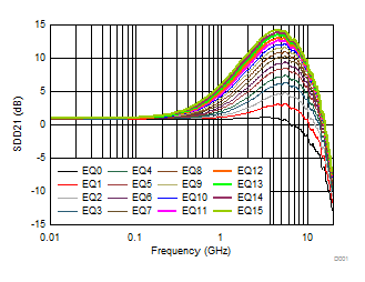
GUID-0223F8E5-FC1C-41C7-8357-BD429BF3C7DD-low.gif
Figure 6-1 DisplayPort EQ Settings Curves
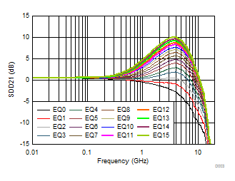
GUID-BA4A6479-5649-418D-8AC1-01808F961BBD-low.gif
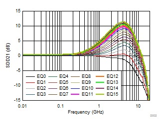
Figure 6-3 USB TX EQ Settings Curves
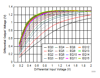
GUID-2BC300C4-B405-4687-811C-6A9EE35EDD30-low.gif
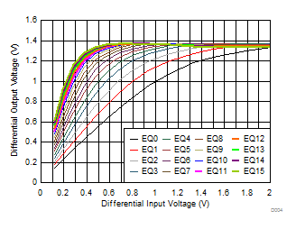
Figure 6-5 USB TX Linearity Curves at 5 GHz
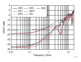
GUID-A6FFD06E-C979-4DA5-BEA0-532330215460-low.gif
Figure 6-7 Input Return Loss Performance
GUID-EC77D24B-C480-42E5-AFBB-00975805907F-low.gif
Figure 6-9 DisplayPort HBR3 Eye-Pattern Performance with 12-inch Input PCB Trace at 8.1 Gbps
GUID-2E378E33-E67D-49F0-97D9-E98C1EE89A00-low.gif
Figure 6-2 USB RX EQ Settings Curves
GUID-B51144E6-525C-4E8B-83EA-6497F5210DCF-low.gif
Figure 6-4 DisplayPort Linearity Curves at 4.05 GHz
GUID-DD42F7AC-C10C-48C2-9BD6-C23B8A47E69D-low.gif
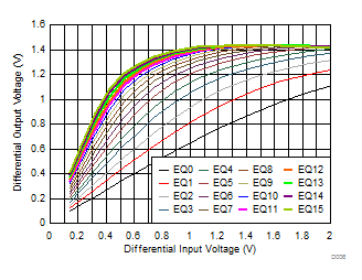
Figure 6-6 USB RX Linearity Curves at 5 GHz
GUID-E61CC225-A534-48EF-955A-90331EDE068A-low.gif
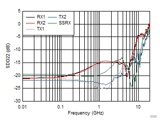
Figure 6-8 Output Return Loss Performance
GUID-3D692004-4E93-466E-9EC8-44CC3E8C7315-low.gif
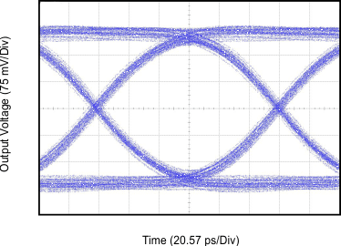
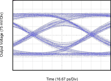
Figure 6-10 USB 3.1 Gen2 Eye-Pattern Performance with 12-inch Input PCB Trace at 10 Gbps