SLLSEZ1C September 2017 – May 2019 TDP142
PRODUCTION DATA.
- 1 Features
- 2 Applications
- 3 Description
- 4 Revision History
- 5 Pin Configuration and Functions
- 6 Specifications
- 7 Parameter Measurement Information
-
8 Detailed Description
- 8.1 Overview
- 8.2 Functional Block Diagram
- 8.3 Feature Description
- 8.4 Device Functional Modes
- 8.5 Programming
- 8.6
Register Maps
- 8.6.1 General Register (address = 0x0A) [reset = 00000001]
- 8.6.2 DisplayPort Control/Status Registers (address = 0x10) [reset = 00000000]
- 8.6.3 DisplayPort Control/Status Registers (address = 0x11) [reset = 00000000]
- 8.6.4 DisplayPort Control/Status Registers (address = 0x12) [reset = 00000000]
- 8.6.5 DisplayPort Control/Status Registers (address = 0x13) [reset = 00000000]
- 9 Application and Implementation
- 10Power Supply Recommendations
- 11Layout
- 12Device and Documentation Support
- 13Mechanical, Packaging, and Orderable Information
9.1 Application Information
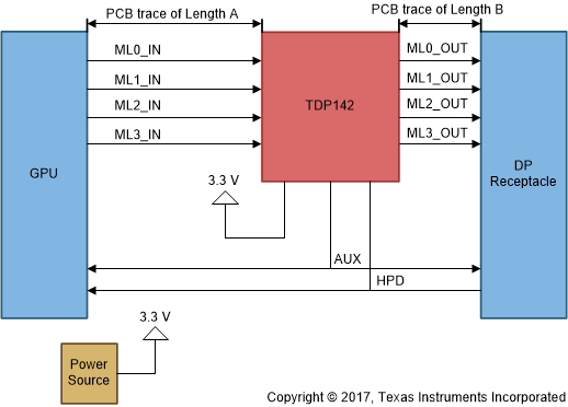
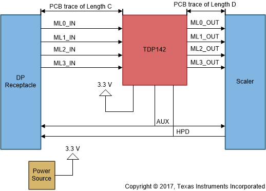
The TDP142 is a linear redriver designed specifically to compensate the inter-symbol interference (ISI) jitter caused by signal attenuation through a passive medium like PCB traces and cable. It can be used in Source, Sink, and cable applications, where the device is transparent to the link training. For illustrating purposes, this section shows the implementations of Source application and Sink application. Figure 16 and Figure 17 are the high level block diagram for DisplayPort Source side application and DisplayPort Sink side application respectively, where the TDP142 is snooping both channels of AUX signal and HPD signal.
 Figure 16. Source Application for TDP142
  Figure 17. The Implementation of Sink Application