SLLSFC5C November 2021 – January 2023 ISOUSB211
PRODUCTION DATA
- 1
- 1 Features
- 2 Applications
- 3 Description
- 4 Revision History
- 5 Pin Configuration and Functions
-
6 Specifications
- 6.1 Absolute Maximum Ratings
- 6.2 ESD Ratings
- 6.3 Recommended Operating Conditions
- 6.4 Thermal Information
- 6.5 Power Ratings
- 6.6 Insulation Specifications
- 6.7 Safety-Related Certifications
- 6.8 Safety Limiting Values
- 6.9 Electrical Characteristics
- 6.10 Switching Characteristics
- 6.11 Insulation Characteristics Curves
- 6.12 Typical Characteristics
- 7 Parameter Measurement Information
-
8 Detailed Description
- 8.1 Overview
- 8.2 Functional Block Diagram
- 8.3
Feature Description
- 8.3.1 Power Supply Options
- 8.3.2 Power Up
- 8.3.3 Symmetric Operation, Dual-Role Port and Role-Reversal
- 8.3.4 Connect and Speed Detection
- 8.3.5 Disconnect Detection
- 8.3.6 Reset
- 8.3.7 LS/FS Message Traffic
- 8.3.8 HS Message Traffic
- 8.3.9 Equalization and Pre-emphasis
- 8.3.10 L2 Power Management State (Suspend) and Resume
- 8.3.11 L1 Power Management State (Sleep) and Resume
- 8.3.12 HS Test Mode Support
- 8.3.13 CDP Advertising
- 8.4 Device Functional Modes
- 9 Power Supply Recommendations
- 10Application and Implementation
- 11Layout
- 12Device and Documentation Support
- 13Mechanical, Packaging, and Orderable Information
13.1 Tape and Reel Information
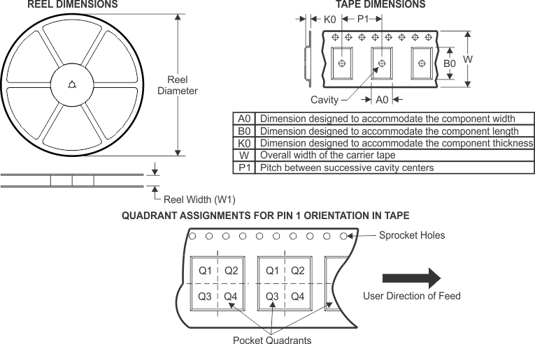
| Device | Package Type |
Package Drawing | Pins | SPQ | Reel Diameter (mm) |
Reel Width W1 (mm) |
A0 (mm) |
B0 (mm) |
K0 (mm) |
P1 (mm) |
W (mm) |
Pin1 Quadrant |
|---|---|---|---|---|---|---|---|---|---|---|---|---|
| ISOUSB211DPR | SSOP | DP | 28 | 2000 | 330.0 | 16.4 | 10.75 | 10.7 | 2.7 | 12.0 | 16.0 | Q1 |
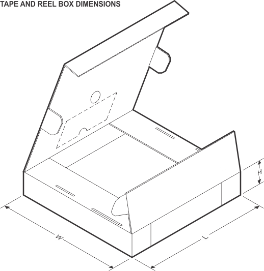
| Device | Package Type | Package Drawing | Pins | SPQ | Length (mm) | Width (mm) | Height (mm) |
|---|---|---|---|---|---|---|---|
| ISOUSB211DPR | SSOP | DP | 28 | 2000 | 350.0 | 350.0 | 43.0 |