SLLSFL4B february 2022 – june 2023 TIOS102 , TIOS1023 , TIOS1025
PRODUCTION DATA
- 1
- 1 Features
- 2 Applications
- 3 Description
- 4 Revision History
- 5 Pin Configuration and Functions
- 6 Specifications
- 7 Parameter Measurement Information
-
8 Detailed Description
- 8.1 Overview
- 8.2 Functional Block Diagrams
- 8.3
Feature Description
- 8.3.1 Current Limit Configuration
- 8.3.2 Current Fault Detection, Indication and Auto Recovery
- 8.3.3 Thermal Warning, Thermal Shutdown
- 8.3.4 Fault Reporting (NFAULT)
- 8.3.5 Device Function Tables
- 8.3.6 The Integrated Voltage Regulator (LDO)
- 8.3.7 Reverse Polarity Protection
- 8.3.8 Integrated Surge Protection and Transient Waveform Tolerance
- 8.3.9 Power Up Sequence
- 8.3.10 Undervoltage Lock-Out (UVLO)
- 8.4 Device Functional Modes
- 9 Application Information Disclaimer
- 10Power Supply Recommendations
- 11Layout
- 12Device and Documentation Support
- 13Mechanical, Packaging, and Orderable Information
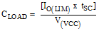
9.2.2.2 Driving Capacitive Loads
These devices are capable of driving capacitive loads on the OUT output. Assuming a pure capacitive load without series/parallel resistance, the maximum capacitance that can be charged without triggering current fault can be calculated as:
To drive higher capacitive loads and avoid overcurrent condition disabling the driver, it is recommended to leave ILIM_ADJ pin floating. With ILIM_ADJ floating, TIOS102(x) indicates overcurrent fault without blanking time delay (tSC) but does not disable the driver. Another approach is to drive high capacitive loads with a series resistor between the output and the load to avoid overcurrent condition. Capacitive loads can be connected to GND or VCC