SLLU149E June 2011 – February 2016 TUSB7320 , TUSB7340
- TUSB73x0 Board Design and Layout Guidelines
- 1 Typical System Implementation
- 2 Power
- 3 Device Reset
- 4 General High Speed Layout Guidelines
- 5 USB Connection
- 6 Package and Breakout
- 7 PCI Express Connection
- 8 Wake from S3
- 9 Device Input Clock
- 10JTAG Interface
- 11Differential Pair ESD Protection
- 12SuperSpeed Redriver
- 13SMI Pin Implementation
- 14Schematics
- Revision History
5.4 SuperSpeed Differential Routing
SuperSpeed consists of two differential routing pairs, a transmit pair (USB_SSTXM and USB_SSTXP) and a receive pair (USB_SSRXM and USB_SSRXP). Each differential pair traces should be routed with 90 Ω ±15% differential impedance. The high-speed signal pair should be trace length matched. Maximum trace length mismatch between SuperSpeed USB signal pairs should be no greater than 5 mils. The total length for each differential pair can be no longer than eight inches, this is based on the SS USB compliance channel spec, and should be avoided if at all possible. TI recommends that the SS diff pairs be as short as possible.
The transmit differential pair does not have to be the same length as the receive differential pair. Keep total trace length to a minimum. Route differential traces first. Route the differential pairs on the top or bottom layers with the minimum amount of vias possible. The transmitter differential pair requires 0.1-µF coupling capacitors for proper operation. The package/case size of these capacitors should be no bigger than 0402. C-packs are not allowed. The capacitors should be placed symmetrically as close as possible to the USB connector signal pins.
If a common mode choke is required, then place the choke as close as possible to the USB connector signal pins (closer than the transmitter capacitors). Likewise, ESD clamps should also be placed as close as possible to the USB connector signal pins (closer than the choke and transmitter capacitors).
It is permissible to swap the plus and minus on either or both of the SuperSpeed differential pairs. This may be necessary to prevent the differential traces from crossing over one another. However it is not permissible to swap the transmitter differential pair with the receive differential pair.
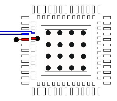
It is recommended to use a 2010 pad for the inside pins provided no pad is used for adjacent pins. Instead use a pad on one of the inside pins then for the next pad route the trace between the outer pins to a via.
There is enough space to route a 3.78-mil trace between the outside pads while leaving 5-mil spacing between the trace and pad, it is then possible to increase the trace width to 4 mils after the breakout. In Figure 5-3 the red pads are USB_SS_RXP/USB_SS_RXN and the blue pads are USB_SS_TXP/USB_SS_TXN.
 Figure 5-3 Differential Routing
 In order to minimize cross-talk on the SS USB differential signal pair, it is recommended that the spacing between the TX and RX signal pairs for each interface be five times the width of the trace (5W rule). For instance, if the SS USB TX differential pair trace width is 5 mils, then there should be 25 mils of space between the TX and RX differential pairs.
If this 5W rule cannot be implemented, then the space between the TX and RX differential pairs should be maximized as much as possible and ground-fill should be placed between the two. In this case, it is better to route each differential pair on opposite sides of the board with a ground plane between them.