SLLU337 June 2021
6 EVM Setup and Operation
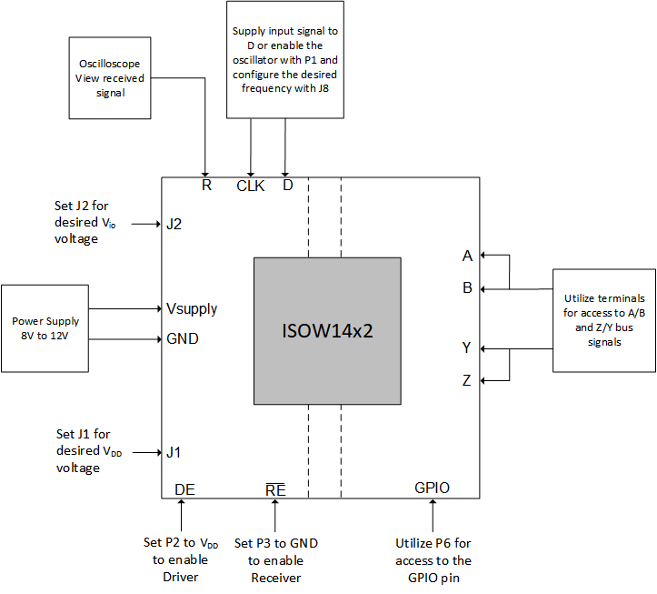
Figure 6-1 shows the basic setup of the EVM with only a single power supply needed to evaluate isolator performance.
Use voltages that are within the range given in the device data sheet. The LDOs on the EVM will provide VDD as configured by their jumpers. The supply voltage to the EVM should ideally be between 8 V and 12 V. ISOW1432 will generate the isolated power for VISOOUT that is connected to VISOOIN on the EVM.
The EVM features an on-board oscillator device that can be used to provide a clock signal to D pin of ISOW1432. The oscillator is bridged to the D input through the Jumper P1 and can be configured to output 12 Mbps or 500 kbps by changing the configuration of J8. Utilizing the on-board oscillator is recommended if conducting any emissions testing on the EVM.
There are two LDOs on the EVM to provide VDD and VIO voltages separately. One can change the LDO output voltage by reconfiguring the jumpers on J1 and J2. J1 controls the output voltage of the LDO supplying VDD and can be 3.3 V or 5 V. J2 controls the output voltage of the LDO supplying Vio and can be 1.8 V, 3.3 V, or 5 V.
J4 and J3 are the terminals that provide access to the A/B and Z/Y bus lines, respectively. These can be used to connect to other RS-485 devices.

Table 6-1 shows the information on jumper configuration for basic tests.
| Connection | Label | Description |
|---|---|---|
| J1 | 3.3 V, 5 V | Connect this jumper to choose the desired VDD voltage of either 3.3 V or 5 V. |
| J2 | 1.8 V, 3.3 V, 5 V | Connect this jumper to choose the desired VIO voltage of 1.8 V, 3.3 V, or 5 V. |
J8 | J8 | Connect this jumper to choose the desired oscillator switching frequency |
P1 | VDD IO, VDD OSC | Connect this jumper to power on and enable the oscillator. |
| P2 | VDD IO, DE, GND1 | Connect this jumper between the middle pin and GND1 to tie the DE pin low. The driver input is disabled when the DE pin is low. Connect this jumper between the middle pin and VDD IO to tie the DE pin high. The driver input is enabled when the DE pin is high. Tie the DE pin to VDD IO for full operation tests. |
P3 | VDD IO, RE, GND1 | Connect this jumper between the middle pin and GND1 to tie the RE pin low. The receiver is enabled when the RE pin is low. Tie the RE pin to GND1 for full operation tests. Connect this jumper between the middle pin and VDD IO to tie the RE pin high. The receiver is disabled when the RE pin is high. |
P7 | VDD IO, EN, GND1 | Connect this jumper between the middle pin and GND1 to disable the DC-DC converter. Leave jumper off or conencted to VDD IO to enable DC-DC converter. |