SLOS417D October 2003 – November 2015 TPA2010D1
PRODUCTION DATA.
- 1 Features
- 2 Applications
- 3 Description
- 4 Device Comparison Table
- 5 Pin Configuration and Functions
- 6 Specifications
- 7 Parameter Measurement Information
- 8 Detailed Description
- 9 Application and Implementation
- 10Power Supply Recommendations
- 11Layout
- 12Device and Documentation Support
- 13Mechanical, Packaging, and Orderable Information
11 Layout
11.1 Layout Guidelines
11.2 Board Layout
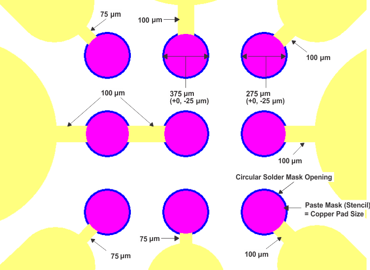
In making the pad size for the DSBGA balls, TI recommends that the layout use nonsolder mask defined (NSMD) land. With this method, the solder mask opening is made larger than the desired land area, and the opening size is defined by the copper pad width. Figure 42 and Table 3 show the appropriate diameters for a DSBGA layout. The TPA2010D1 evaluation module (EVM) layout is shown in the next section as a layout example.
Follow these guidelines:
- Circuit traces from NSMD defined PWB lands should be 75 µm to 100 µm wide in the exposed area inside the solder mask opening. Wider trace widths reduce device stand off and impact reliability.
- Recommend solder paste is Type 3 or Type 4.
- Best reilability results are achieved when the PWB laminate glass transition temperature is above the operating the range of the intended application.
- For a PWB using a Ni/Au surface finish, the gold thickness should be less 0.5 µm to avoid a reduction in thermal fatigue performance.
- Solder mask thickness should be less than 20 µm on top of the copper circuit pattern.
- Best solder stencil performance is achieved using laser cut stencils with electro polishing. Use of chemically etched stencils results in inferior solder paste volume control.
- Trace routing away from DSBGA device should be balanced in X and Y directions to avoid unintentional component movement due to solder wetting forces.
11.2.1 Component Location
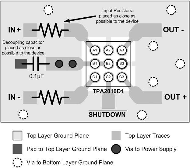
Place all the external components very close to the TPA2010D1. The input resistors need to be very close to the TPA2010D1 input pins so noise does not couple on the high impedance nodes between the input resistors and the input amplifier of the TPA2010D1. Placing the decoupling capacitor, CS, close to the TPA2010D1 is important for the efficiency of the class-D amplifier. Any resistance or inductance in the trace between the device and the capacitor can cause a loss in efficiency.
11.2.2 Trace Width
Recommended trace width at the solder balls is 75 µm to 100 µm to prevent solder wicking onto wider PCB traces. Figure 40 shows the layout of the TPA2010D1 evaluation module (EVM).
For high current pins (VDD, GND VO+, and VO–) of the TPA2010D1, use 100-µm trace widths at the solder balls and at least 500-µm PCB traces to ensure proper performance and output power for the device.
For input pins (IN–, IN+, and SHUTDOWN) of the TPA2010D1, use 75-µm to 100-µm trace widths at the solder balls. IN– and IN+ pins need to run side-by-side to maximize common-mode noise cancellation. Placing input resistors, RIN, as close to the TPA2010D1 as possible is recommended.
 Figure 40. Close Up of TPA2010D1 Land Pattern from TPA2010D1 EVM
11.3 Layout Example
 Figure 41. TPA2010D1 Layout Example