SLOS782C July 2013 – May 2017 TAS5760L
PRODUCTION DATA.
- 1 Features
- 2 Applications
- 3 Description
- 4 Revision History
- 5 Device Comparison Table
- 6 Pin Configuration and Functions
-
7 Specifications
- 7.1 Absolute Maximum Ratings
- 7.2 ESD Ratings
- 7.3 Recommended Operating Conditions
- 7.4 Thermal Information
- 7.5 Digital I/O Pins
- 7.6 Master Clock
- 7.7 Serial Audio Port
- 7.8 Protection Circuitry
- 7.9 Speaker Amplifier in All Modes
- 7.10 Speaker Amplifier in Stereo Bridge-Tied Load (BTL) Mode
- 7.11 Speaker Amplifier in Mono Parallel Bridge-Tied Load (PBTL) Mode
- 7.12 I²C Control Port
- 7.13 Typical Idle, Mute, Shutdown, Operational Power Consumption
- 7.14 Typical Speaker Amplifier Performance Characteristics (Stereo BTL Mode)
- 7.15 Typical Performance Characteristics (Mono PBTL Mode)
- 8 Parameter Measurement Information
-
9 Detailed Description
- 9.1 Overview
- 9.2 Functional Block Diagram
- 9.3 Feature Description
- 9.4
Device Functional Modes
- 9.4.1
Hardware Control Mode
- 9.4.1.1 Speaker Amplifier Shut Down (SPK_SD Pin)
- 9.4.1.2 Serial Audio Port in Hardware Control Mode
- 9.4.1.3 Soft Clipper Control (SFT_CLIP Pin)
- 9.4.1.4 Speaker Amplifier Switching Frequency Select (FREQ/SDA Pin)
- 9.4.1.5 Parallel Bridge Tied Load Mode Select (PBTL/SCL Pin)
- 9.4.1.6 Speaker Amplifier Sleep Enable (SPK_SLEEP/ADR Pin)
- 9.4.1.7 Speaker Amplifier Gain Select (SPK_GAIN [1:0] Pins)
- 9.4.1.8 Considerations for Setting the Speaker Amplifier Gain Structure
- 9.4.2 Software Control Mode
- 9.4.1
Hardware Control Mode
- 9.5
Register Maps
- 9.5.1 Control Port Registers - Quick Reference
- 9.5.2
Control Port Registers - Detailed Description
- 9.5.2.1 Device Identification Register (0x00)
- 9.5.2.2 Power Control Register (0x01)
- 9.5.2.3 Digital Control Register (0x02)
- 9.5.2.4 Volume Control Configuration Register (0x03)
- 9.5.2.5 Left Channel Volume Control Register (0x04)
- 9.5.2.6 Right Channel Volume Control Register (0x05)
- 9.5.2.7 Analog Control Register (0x06)
- 9.5.2.8 Reserved Register (0x07)
- 9.5.2.9 Fault Configuration and Error Status Register (0x08)
- 9.5.2.10 Reserved Controls (9 / 0x09) - (15 / 0x0F)
- 9.5.2.11 Digital Clipper Control 2 Register (0x10)
- 9.5.2.12 Digital Clipper Control 1 Register (0x11)
-
10Application and Implementation
- 10.1 Application Information
- 10.2
Typical Applications
- 10.2.1 Stereo BTL Using Software Control
- 10.2.2 Stereo BTL Using Hardware Control
- 10.2.3 Mono PBTL Using Software Control
- 10.2.4 Mono PBTL Using Hardware Control
- 10.2.5 Stereo BTL Using Software Control, 32-Pin DAP Package Option
- 10.2.6 Stereo BTL Using Hardware Control, 32-Pin DAP Package Option
- 10.2.7 Mono PBTL Using Software Control, 32-Pin DAP Package Option
- 10.2.8 Mono PBTL Using Hardware Control, 32-Pin DAP Package Option
- 11Power Supply Recommendations
- 12Layout
- 13Device and Documentation Support
- 14Mechanical, Packaging, and Orderable Information
10 Application and Implementation
NOTE
Information in the following applications sections is not part of the TI component specification, and TI does not warrant its accuracy or completeness. TI’s customers are responsible for determining suitability of components for their purposes. Customers should validate and test their design implementation to confirm system functionality.
10.1 Application Information
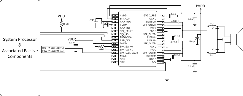
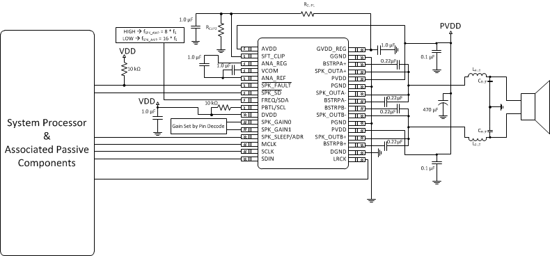
These typical connection diagrams highlight the required external components and system level connections for proper operation of the device in several popular use cases.
Each of these configurations can be realized using the Evaluation Modules (EVMs) for the device. These flexible modules allow full evaluation of the device in all available modes of operation. Additionally, some of the application circuits are available as reference designs and can be found on the TI website. Also see the TAS5760L's product page for information on ordering the EVM. Not all configurations are available as reference designs; however, any design variation can be supported by TI through schematic and layout reviews. Visit support.ti.com for additional design assistance. Also, join the audio amplifier discussion forum at http://e2e.ti.com.
10.2 Typical Applications
These application circuits detail the recommended component selection and board configurations for the TAS5760L device. Note that in Software Control mode, the clipping point of the amplifier and thus the rated power of the end equipment can be set using the digital clipper if desired. Additionally, if the sonic signature of the soft clipper is preferred, it can be used in addition to or in lieu of the digital clipper. The software control application circuit detailed in this section shows the soft clipper in its bypassed state, which results in a lower BOM count than when using the soft clipper. The trade-off between the sonic characteristics of the clipping events in the amplifier and BOM minimization can be chosen based upon the design goals related to the end product.
10.2.1 Stereo BTL Using Software Control
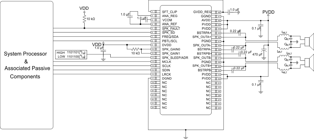 Figure 57. Stereo BTL Using Software Control
10.2.1.1 Design Requirements
For this design example, use the parameters listed in Table 19 as the input parameters.
10.2.1.2 Detailed Design Procedure
10.2.1.2.1 Startup Procedures- Software Control Mode
- Configure all digital I/O pins as required by the application using PCB connections (that is SPK_GAIN[1:0] = 11, ADR, etc.)
- Start with SPK_SD Pin = LOW
- Bring up power supplies (it does not matter if PVDD/AVDD or DVDD comes up first, provided the device is held in shutdown.)
- Once power supplies are stable, start MCLK, SCLK, LRCK
- Configure the device via the control port in the manner required by the use case, making sure to mute the device via the control port
- Once power supplies and clocks are stable and the control port has been programmed, bring SPK_SD HIGH
- Unmute the device via the control port
- The device is now in normal operation
NOTE
Control port register changes should only occur when the device is placed into shutdown. This can be accomplished either by pulling the SPK_SD pin LOW or clearing the SPK_SD bit in the control port.
10.2.1.2.2 Shutdown Procedures- Software Control Mode
- The device is in normal operation
- Mute via the control port
- Pull SPK_SD LOW
- The clocks can now be stopped and the power supplies brought down
- The device is now fully shutdown and powered off
NOTE
Any control port register changes excluding volume control changes should only occur when the device is placed into shutdown. This can be accomplished either by pulling the SPK_SD pin LOW or clearing the SPK_SD bit in the control port.
10.2.1.2.3 Component Selection and Hardware Connections
details the typical connections required for proper operation of the device. It is with this list of components that the device was simulated, tested, and characterized. Deviation from this typical application circuit unless recommended by this document may produce unwanted results, which could range from degradation of audio performance to destructive failure of the device.
10.2.1.2.3.1 I²C Pullup Resistors
It is important to note that when the device is operated in Software Control Mode, the customary pullup resistors are required on the SCL and SDA signal lines. They are not shown in the Typical Application Circuits, because they are shared by all of the devices on the I²C bus and are considered to be part of the associated passive components for the System Processor. These resistor values should be chosen per the guidance provided in the I²C Specification.
10.2.1.2.3.2 Digital I/O Connectivity
The digital I/O lines of the TAS5760L are described in previous sections. As discussed, whenever a static digital pin (that is a pin that is hardwired to be HIGH or LOW) is required to be pulled HIGH, it should be connected to DVDD through a pullup resistor to control the slew rate of the voltage presented to the digital I/O pins. It is not, however, necessary to have a separate pullup resistor for each static digital I/O line. Instead, a single resistor can be used to tie all static I/O lines HIGH to reduce BOM count. For instance, if Software Control Mode is desired both the GAIN[1:0] and the PBTL/SCL pins can both be pulled HIGH through a single pullup resistor.
10.2.1.2.4 Recommended Startup and Shutdown Procedures
The start up and shutdown procedures for both Hardware Control Mode and Software Control Mode are shown below.
10.2.1.3 Application Curve
Table 20. Relevant Performance Plots
| PLOT TITLE | PLOT NUMBER |
|---|---|
| Figure 1. Output Power vs PVDD | G001 |
| Figure 2. THD+N vs Frequency With PVDD = 12 V, POSPK = 1 W | G024 |
| Figure 5. THD+N vs Output Power With PVDD = 12 V, Both Channels Driven | G027 |
| Figure 7. Efficiency vs Output Power | G030 |
| Figure 8. Crosstalk vs Frequency | G031 |
| Figure 9. PVDD PSRR vs Frequency | G019 |
| Figure 10. DVDD PSRR vs Frequency | G020 |
| Figure 11. Idle Current Draw vs PVDD (Filterless) | G042 |
| Figure 12. Idle Current Draw vs PVDD (With LC Filter as Shown on the EVM) | G023 |
| Figure 13. Shutdown Current Draw vs PVDD (Filterless) | G022 |
| Figure 14. Output Power vs PVDD | G039 |
| Figure 15. THD+N vs Frequency With PVDD = 12 V, POSPK = 1 W | G002 |
| Figure 18. THD+N vs Output Power With PVDD = 12 V, Both Channels Driven | G008 |
| Figure 20. Efficiency vs Output Power | G014 |
| Figure 21. Crosstalk vs Frequency | G018 |
| Figure 22. PVDD PSRR vs Frequency | G019 |
| Figure 23. Idle Current Draw vs PVDD (Filterless) | G045 |
| Figure 24. Idle Current Draw vs PVDD (With LC Filter as Shown on EVM) | G044 |
| Figure 25. Shutdown Current Draw vs PVDD (Filterless) | G022 |
10.2.2 Stereo BTL Using Hardware Control
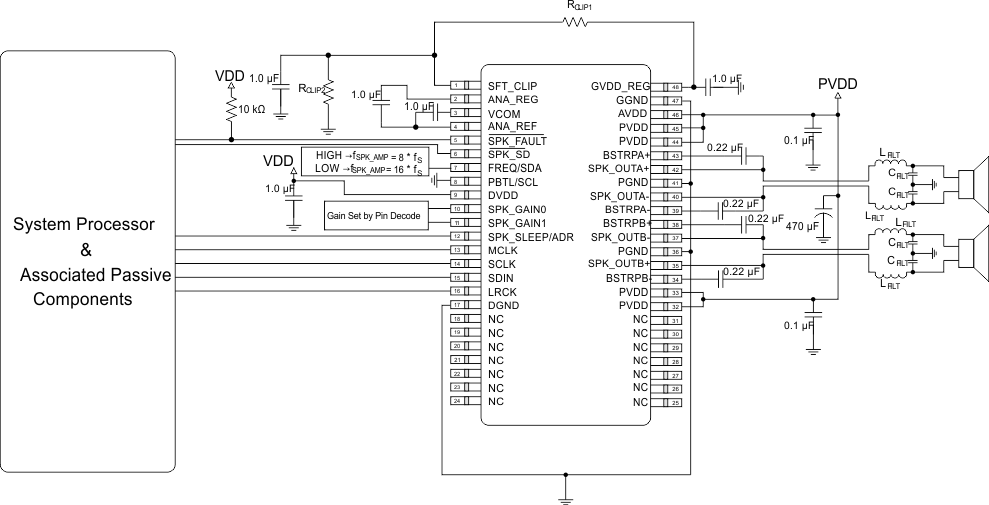 Figure 58. Stereo BTL Using Hardware Control
10.2.2.1 Design Requirements
For this design example, use the parameters listed in Table 21 as the input parameters.
10.2.2.2 Detailed Design Procedure
10.2.2.2.1 Startup Procedures- Hardware Control Mode
- Configure all hardware pins as required by the application using PCB connections (that is PBTL, FREQ, GAIN, etc.)
- Start with SPK_SD pin pulled LOW and SPK_SLEEP/ADR pin pulled HIGH
- Bring up power supplies (it does not matter if PVDD/AVDD or DVDD comes up first, provided the device is held in shutdown.)
- Once power supplies are stable, start MCLK, SCLK, LRCK
- Once power supplies and clocks are stable and all hardware control pins have been configured, bring SPK_SD HIGH
- Once the device is out of shutdown mode, bring SPK_SLEEP/ADR LOW
- The device is now in normal operation
10.2.2.2.2 Shutdown Procedures- Hardware Control Mode
- The device is in normal operation
- Pull SPK_SLEEP/ADR HIGH
- Pull SPK_SD LOW
- The clocks can now be stopped and the power supplies brought down
- The device is now fully shutdown and powered off
10.2.2.2.3 Digital I/O Connectivity
The digital I/O lines of the TAS5760L are described in previous sections. As discussed, whenever a static digital pin (that is a pin that is hardwired to be HIGH or LOW) is required to be pulled HIGH, it should be connected to DVDD through a pullup resistor in order to control the slew rate of the voltage presented to the digital I/O pins. It is not, however, necessary to have a separate pullup resistor for each static digital I/O line. Instead, a single resistor can be used to tie all static I/O lines HIGH to reduce BOM count. For instance, if Software Control Mode is desired both the GAIN[1:0] and the PBTL/SCL pins can both be pulled HIGH through a single pullup resistor.
10.2.2.3 Application Curve
Table 22. Relevant Performance Plots
| PLOT TITLE | PLOT NUMBER |
|---|---|
| Figure 1. Output Power vs PVDD | G001 |
| Figure 2. THD+N vs Frequency With PVDD = 12 V, POSPK = 1 W | G024 |
| Figure 4. Idle Channel Noise vs PVDD | G026 |
| Figure 5. THD+N vs Output Power With PVDD = 12 V, Both Channels Driven | G027 |
| Figure 7. Efficiency vs Output Power | G030 |
| Figure 8. Crosstalk vs Frequency | G031 |
| Figure 9. PVDD PSRR vs Frequency | G019 |
| Figure 10. DVDD PSRR vs Frequency | G020 |
| Figure 11. Idle Current Draw vs PVDD (Filterless) | G042 |
| Figure 12. Idle Current Draw vs PVDD (With LC Filter as Shown on the EVM) | G023 |
| Figure 13. Shutdown Current Draw vs PVDD (Filterless) | G022 |
| Figure 14. Output Power vs PVDD | G039 |
| Figure 15. THD+N vs Frequency With PVDD = 12 V, POSPK = 1 W | G002 |
| Figure 17. Idle Channel Noise vs PVDD | G006 |
| Figure 18. THD+N vs Output Power With PVDD = 12 V, Both Channels Driven | G008 |
| Figure 20. Efficiency vs Output Power | G014 |
| Figure 21. Crosstalk vs Frequency | G018 |
| Figure 22. PVDD PSRR vs Frequency | G019 |
| Figure 23. Idle Current Draw vs PVDD (Filterless) | G045 |
| Figure 24. Idle Current Draw vs PVDD (With LC Filter as Shown on EVM) | G044 |
| Figure 25. Shutdown Current Draw vs PVDD (Filterless) | G022 |
10.2.3 Mono PBTL Using Software Control
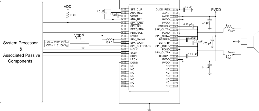 Figure 59. Mono PBTL Using Software Control
10.2.3.1 Design Requirements
For this design example, use the parameters listed in Table 23 as the input parameters.
10.2.3.2 Detailed Design Procedure
10.2.3.2.1 Startup Procedures- Software Control Mode
- Configure all digital I/O pins as required by the application using PCB connections (that is SPK_GAIN[1:0] = 11, ADR, etc.)
- Start with SPK_SD Pin = LOW
- Bring up power supplies (it does not matter if PVDD/AVDD or DVDD comes up first, provided the device is held in shutdown.)
- Once power supplies are stable, start MCLK, SCLK, LRCK
- Configure the device via the control port in the manner required by the use case, making sure to mute the device via the control port
- Once power supplies and clocks are stable and the control port has been programmed, bring SPK_SD HIGH
- Unmute the device via the control port
- The device is now in normal operation
NOTE
Control port register changes should only occur when the device is placed into shutdown. This can be accomplished either by pulling the SPK_SD pin LOW or clearing the SPK_SD bit in the control port.
10.2.3.2.2 Shutdown Procedures- Software Control Mode
- The device is in normal operation
- Mute via the control port
- Pull SPK_SD LOW
- The clocks can now be stopped and the power supplies brought down
- The device is now fully shutdown and powered off
NOTE
Any control port register changes excluding volume control changes should only occur when the device is placed into shutdown. This can be accomplished either by pulling the SPK_SD pin LOW or clearing the SPK_SD bit in the control port.
10.2.3.2.3 Component Selection and Hardware Connections
above details the typical connections required for proper operation of the device. It is with this list of components that the device was simulated, tested, and characterized. Deviation from this typical application circuit unless recommended by this document may produce unwanted results, which could range from degradation of audio performance to destructive failure of the device.
10.2.3.2.3.1 I²C Pull-Up Resistors
It is important to note that when the device is operated in Software Control Mode, the customary pull-up resistors are required on the SCL and SDA signal lines. They are not shown in the Typical Application Circuits, since they are shared by all of the devices on the I²C bus and are considered to be part of the associated passive components for the System Processor. These resistor values should be chosen per the guidance provided in the I²C Specification.
10.2.3.2.3.2 Digital I/O Connectivity
The digital I/O lines of the TAS5760L are described in previous sections. As discussed, whenever a static digital pin (that is a pin that is hardwired to be HIGH or LOW) is required to be pulled HIGH, it should be connected to DVDD through a pullup resistor in order to control the slew rate of the voltage presented to the digital I/O pins. It is not, however, necessary to have a separate pullup resistor for each static digital I/O line. Instead, a single resistor can be used to tie all static I/O lines HIGH to reduce BOM count. For instance, if Software Control Mode is desired both the GAIN[1:0] and the PBTL/SCL pins can both be pulled HIGH through a single pullup resistor.
10.2.3.3 Application Curve
Table 24. Relevant Performance Plots
| PLOT TITLE | PLOT NUMBER |
|---|---|
| Figure 27. THD+N vs Frequency With PVDD = 12 V, POSPK = 1 W | G032 |
| Figure 29. THD+N vs Output Power With PVDD = 12 V With 1 kHz Sine Input | G035 |
| Figure 37. Efficiency vs Output Power | G038 |
| Figure 2. THD+N vs Frequency With PVDD = 12 V, POSPK = 1 W | G004 |
| Figure 35. THD+N vs Output Power With PVDD = 12 V | G011 |
| Figure 7. Efficiency vs Output Power | G015 |
10.2.4 Mono PBTL Using Hardware Control
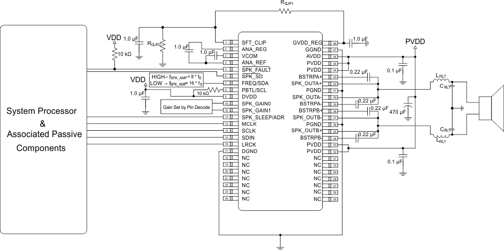 Figure 60. Mono PBTL Using Hardware Control
10.2.4.1 Design Requirements
For this design example, use the parameters listed in Table 25 as the input parameters.
10.2.4.2 Detailed Design Procedure
10.2.4.2.1 Startup Procedures- Hardware Control Mode
- Configure all hardware pins as required by the application using PCB connections (that is PBTL, FREQ, GAIN, etc.)
- Start with SPK_SD pin pulled LOW and SPK_SLEEP/ADR pin pulled HIGH
- Bring up power supplies (it does not matter if PVDD/AVDD or DVDD comes up first, provided the device is held in shutdown.)
- Once power supplies are stable, start MCLK, SCLK, LRCK
- Once power supplies and clocks are stable and all hardware control pins have been configured, bring SPK_SD HIGH
- Once the device is out of shutdown mode, bring SPK_SLEEP/ADR LOW
- The device is now in normal operation
10.2.4.2.2 Shutdown Procedures- Hardware Control Mode
- The device is in normal operation
- Pull SPK_SLEEP/ADR HIGH
- Pull SPK_SD LOW
- The clocks can now be stopped and the power supplies brought down
- The device is now fully shutdown and powered off
10.2.4.2.3 Component Selection and Hardware Connections
details the typical connections required for proper operation of the device. It is with this list of components that the device was simulated, tested, and characterized. Deviation from this typical application circuit unless recommended by this document may produce unwanted results, which could range from degradation of audio performance to destructive failure of the device.
10.2.4.2.4 Digital I/O Connectivity
The digital I/O lines of the TAS5760L are described in previous sections. As discussed, whenever a static digital pin (that is a pin that is hardwired to be HIGH or LOW) is required to be pulled HIGH, it should be connected to DVDD through a pullup resistor in order to control the slew rate of the voltage presented to the digital I/O pins. It is not, however, necessary to have a separate pullup resistor for each static digital I/O line. Instead, a single resistor can be used to tie all static I/O lines HIGH to reduce BOM count. For instance, if Software Control Mode is desired both the GAIN[1:0] and the PBTL/SCL pins can both be pulled HIGH through a single pullup resistor.
10.2.4.3 Application Curve
Table 26. Relevant Performance Plots
| PLOT TITLE | PLOT NUMBER |
|---|---|
| Figure 32. THD+N vs Frequency With PVDD = 12 V, POSPK = 1 W | G032 |
| Figure 34. Idle Channel Noise vs PVDD | G034 |
| Figure 29. THD+N vs Output Power With PVDD = 12 V With 1 kHz Sine Input | G035 |
| Figure 37. Efficiency vs Output Power | G038 |
| Figure 2. THD+N vs Frequency With PVDD = 12 V, POSPK = 1 W | G004 |
| Figure 17. Idle Channel Noise vs PVDD | G007 |
| Figure 35. THD+N vs Output Power With PVDD = 12 V | G011 |
| Figure 7. Efficiency vs Output Power | G015 |
10.2.5 Stereo BTL Using Software Control, 32-Pin DAP Package Option
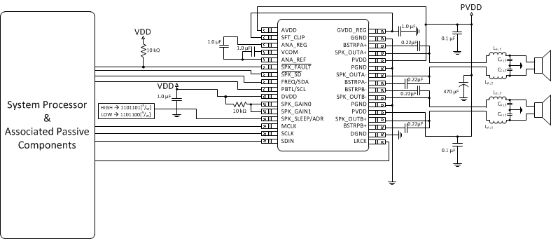 Figure 61. Stereo BTL using Software Control, 32-Pin DAP Package Option
10.2.5.1 Design Requirements
For this design example, use the parameters listed in Table 27 as the input parameters.
10.2.5.2 Detailed Design Procedure
10.2.5.2.1 Startup Procedures- Software Control Mode
- Configure all digital I/O pins as required by the application using PCB connections (that is SPK_GAIN[1:0] = 11, ADR, etc.)
- Start with SPK_SD Pin = LOW
- Bring up power supplies (it does not matter if PVDD/AVDD or DVDD comes up first, provided the device is held in shutdown.)
- Once power supplies are stable, start MCLK, SCLK, LRCK
- Configure the device via the control port in the manner required by the use case, making sure to mute the device via the control port
- Once power supplies and clocks are stable and the control port has been programmed, bring SPK_SD HIGH
- Unmute the device via the control port
- The device is now in normal operation
NOTE
Control port register changes should only occur when the device is placed into shutdown. This can be accomplished either by pulling the SPK_SD pin LOW or clearing the SPK_SD bit in the control port.
10.2.5.2.2 Shutdown Procedures- Software Control Mode
- The device is in normal operation
- Mute via the control port
- Pull SPK_SD LOW
- The clocks can now be stopped and the power supplies brought down
- The device is now fully shutdown and powered off
NOTE
Any control port register changes excluding volume control changes should only occur when the device is placed into shutdown. This can be accomplished either by pulling the SPK_SD pin LOW or clearing the SPK_SD bit in the control port.
10.2.5.2.3 Component Selection and Hardware Connections
Figure 61 details the typical connections required for proper operation of the device. It is with this list of components that the device was simulated, tested, and characterized. Deviation from this typical application circuit unless recommended by this document may produce unwanted results, which could range from degradation of audio performance to destructive failure of the device.
10.2.5.2.3.1 I²C Pullup Resistors
It is important to note that when the device is operated in Software Control Mode, the customary pullup resistors are required on the SCL and SDA signal lines. They are not shown in the Typical Application Circuits, because they are shared by all of the devices on the I²C bus and are considered to be part of the associated passive components for the System Processor. These resistor values should be chosen per the guidance provided in the I²C Specification.
10.2.5.2.3.2 Digital I/O Connectivity
The digital I/O lines of the TAS5760L are described in previous sections. As discussed, whenever a static digital pin (that is a pin that is hardwired to be HIGH or LOW) is required to be pulled HIGH, it should be connected to DVDD through a pullup resistor to control the slew rate of the voltage presented to the digital I/O pins. It is not, however, necessary to have a separate pullup resistor for each static digital I/O line. Instead, a single resistor can be used to tie all static I/O lines HIGH to reduce BOM count. For instance, if Software Control Mode is desired both the GAIN[1:0] and the PBTL/SCL pins can both be pulled HIGH through a single pullup resistor.
10.2.5.2.4 Recommended Startup and Shutdown Procedures
The start up and shutdown procedures for both Hardware Control Mode and Software Control Mode are shown below.
10.2.5.3 Application Curve
Table 28. Relevant Performance Plots
| PLOT TITLE | PLOT NUMBER |
|---|---|
| Figure 1. Output Power vs PVDD | G001 |
| Figure 2. THD+N vs Frequency With PVDD = 12 V, POSPK = 1 W | G024 |
| Figure 5. THD+N vs Output Power With PVDD = 12 V, Both Channels Driven | G027 |
| Figure 7. Efficiency vs Output Power | G030 |
| Figure 8. Crosstalk vs Frequency | G031 |
| Figure 22. PVDD PSRR vs Frequency | G019 |
| Figure 10. DVDD PSRR vs Frequency | G020 |
| Figure 11. Idle Current Draw vs PVDD (Filterless) | G042 |
| Figure 12. Idle Current Draw vs PVDD (With LC Filter as Shown on the EVM) | G023 |
| Figure 13. Shutdown Current Draw vs PVDD (Filterless) | G022 |
| Figure 14. Output Power vs PVDD | G039 |
| Figure 15. THD+N vs Frequency With PVDD = 12 V, POSPK = 1 W | G002 |
| Figure 18. THD+N vs Output Power With PVDD = 12 V, Both Channels Driven | G008 |
| Figure 7. Efficiency vs Output Power | G014 |
| Figure 21. Crosstalk vs Frequency | G018 |
| Figure 22. PVDD PSRR vs Frequency | G019 |
| Figure 23. Idle Current Draw vs PVDD (Filterless) | G045 |
| Figure 24. Idle Current Draw vs PVDD (With LC Filter as Shown on EVM) | G044 |
| Figure 25. Shutdown Current Draw vs PVDD (Filterless) | G022 |
10.2.6 Stereo BTL Using Hardware Control, 32-Pin DAP Package Option
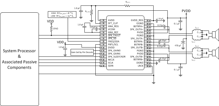 Figure 62. Stereo BTL using Hardware Control, 32-Pin DAP Package Option
10.2.6.1 Design Requirements
For this design example, use the parameters listed in Table 29 as the input parameters.
10.2.6.2 Detailed Design Procedure
10.2.6.2.1 Startup Procedures- Hardware Control Mode
- Configure all hardware pins as required by the application using PCB connections (that is PBTL, FREQ, GAIN, etc.)
- Start with SPK_SD pin pulled LOW and SPK_SLEEP/ADR pin pulled HIGH
- Bring up power supplies (it does not matter if PVDD/AVDD or DVDD comes up first, provided the device is held in shutdown.)
- Once power supplies are stable, start MCLK, SCLK, LRCK
- Once power supplies and clocks are stable and all hardware control pins have been configured, bring SPK_SD HIGH
- Once the device is out of shutdown mode, bring SPK_SLEEP/ADR LOW
- The device is now in normal operation
10.2.6.2.2 Shutdown Procedures- Hardware Control Mode
- The device is in normal operation
- Pull SPK_SLEEP/ADR HIGH
- Pull SPK_SD LOW
- The clocks can now be stopped and the power supplies brought down
- The device is now fully shutdown and powered off
10.2.6.2.3 Digital I/O Connectivity
The digital I/O lines of the TAS5760L are described in previous sections. As discussed, whenever a static digital pin (that is a pin that is hardwired to be HIGH or LOW) is required to be pulled HIGH, it should be connected to DVDD through a pullup resistor in order to control the slew rate of the voltage presented to the digital I/O pins. It is not, however, necessary to have a separate pullup resistor for each static digital I/O line. Instead, a single resistor can be used to tie all static I/O lines HIGH to reduce BOM count. For instance, if Software Control Mode is desired both the GAIN[1:0] and the PBTL/SCL pins can both be pulled HIGH through a single pullup resistor.
10.2.6.3 Application Curve
Table 30. Relevant Performance Plots
| PLOT TITLE | PLOT NUMBER |
|---|---|
| Figure 1. Output Power vs PVDD | G001 |
| Figure 2. THD+N vs Frequency With PVDD = 12 V, POSPK = 1 W | G024 |
| Figure 4. Idle Channel Noise vs PVDD | G026 |
| Figure 5. THD+N vs Output Power With PVDD = 12 V, Both Channels Driven | G027 |
| Figure 7. Efficiency vs Output Power | G030 |
| Figure 8. Crosstalk vs Frequency | G031 |
| Figure 22. PVDD PSRR vs Frequency | G019 |
| Figure 10. DVDD PSRR vs Frequency | G020 |
| Figure 11. Idle Current Draw vs PVDD (Filterless) | G042 |
| Figure 12. Idle Current Draw vs PVDD (With LC Filter as Shown on the EVM) | G023 |
| Figure 13. Shutdown Current Draw vs PVDD (Filterless) | G022 |
| Figure 14. Output Power vs PVDD | G039 |
| Figure 15. THD+N vs Frequency With PVDD = 12 V, POSPK = 1 W | G002 |
| Figure 17. Idle Channel Noise vs PVDD | G006 |
| Figure 18. THD+N vs Output Power With PVDD = 12 V, Both Channels Driven | G008 |
| Figure 7. Efficiency vs Output Power | G014 |
| Figure 21. Crosstalk vs Frequency | G018 |
| Figure 22. PVDD PSRR vs Frequency | G019 |
| Figure 23. Idle Current Draw vs PVDD (Filterless) | G045 |
| Figure 24. Idle Current Draw vs PVDD (With LC Filter as Shown on EVM) | G044 |
| Figure 25. Shutdown Current Draw vs PVDD (Filterless) | G022 |
10.2.7 Mono PBTL Using Software Control, 32-Pin DAP Package Option
10.2.7.1 Design Requirements
For this design example, use the parameters listed in Table 31 as the input parameters.
10.2.7.2 Detailed Design Procedure
10.2.7.2.1 Startup Procedures- Software Control Mode
- Configure all digital I/O pins as required by the application using PCB connections (that is SPK_GAIN[1:0] = 11, ADR, etc.)
- Start with SPK_SD Pin = LOW
- Bring up power supplies (it does not matter if PVDD/AVDD or DVDD comes up first, provided the device is held in shutdown.)
- Once power supplies are stable, start MCLK, SCLK, LRCK
- Configure the device via the control port in the manner required by the use case, making sure to mute the device via the control port
- Once power supplies and clocks are stable and the control port has been programmed, bring SPK_SD HIGH
- Unmute the device via the control port
- The device is now in normal operation
NOTE
Control port register changes should only occur when the device is placed into shutdown. This can be accomplished either by pulling the SPK_SD pin LOW or clearing the SPK_SD bit in the control port.
10.2.7.2.2 Shutdown Procedures- Software Control Mode
- The device is in normal operation
- Mute via the control port
- Pull SPK_SD LOW
- The clocks can now be stopped and the power supplies brought down
- The device is now fully shutdown and powered off
NOTE
Any control port register changes excluding volume control changes should only occur when the device is placed into shutdown. This can be accomplished either by pulling the SPK_SD pin LOW or clearing the SPK_SD bit in the control port.
10.2.7.2.3 Component Selection and Hardware Connections
Figure 63 above details the typical connections required for proper operation of the device. It is with this list of components that the device was simulated, tested, and characterized. Deviation from this typical application circuit unless recommended by this document may produce unwanted results, which could range from degradation of audio performance to destructive failure of the device.
10.2.7.2.3.1 I²C Pull-Up Resistors
It is important to note that when the device is operated in Software Control Mode, the customary pull-up resistors are required on the SCL and SDA signal lines. They are not shown in the Typical Application Circuits, since they are shared by all of the devices on the I²C bus and are considered to be part of the associated passive components for the System Processor. These resistor values should be chosen per the guidance provided in the I²C Specification.
10.2.7.2.3.2 Digital I/O Connectivity
The digital I/O lines of the TAS5760L are described in previous sections. As discussed, whenever a static digital pin (that is a pin that is hardwired to be HIGH or LOW) is required to be pulled HIGH, it should be connected to DVDD through a pullup resistor in order to control the slew rate of the voltage presented to the digital I/O pins. It is not, however, necessary to have a separate pullup resistor for each static digital I/O line. Instead, a single resistor can be used to tie all static I/O lines HIGH to reduce BOM count. For instance, if Software Control Mode is desired both the GAIN[1:0] and the PBTL/SCL pins can both be pulled HIGH through a single pullup resistor.
10.2.7.3 Application Curve
Table 32. Relevant Performance Plots
| PLOT TITLE | PLOT NUMBER |
|---|---|
| Figure 2. THD+N vs Frequency With PVDD = 12 V, POSPK = 1 W | G032 |
| Figure 29. THD+N vs Output Power With PVDD = 12 V With 1 kHz Sine Input | G035 |
| Figure 7. Efficiency vs Output Power | G038 |
| Figure 16. THD+N vs Frequency With PVDD = 12 V, POSPK = 1 W | G004 |
| Figure 35. THD+N vs Output Power With PVDD = 12 V | G011 |
| Figure 31. Efficiency vs Output Power | G015 |
10.2.8 Mono PBTL Using Hardware Control, 32-Pin DAP Package Option
10.2.8.1 Design Requirements
For this design example, use the parameters listed in Table 33 as the input parameters.
10.2.8.2 Detailed Design Procedure
10.2.8.2.1 Startup Procedures- Hardware Control Mode
- Configure all hardware pins as required by the application using PCB connections (that is PBTL, FREQ, GAIN, etc.)
- Start with SPK_SD pin pulled LOW and SPK_SLEEP/ADR pin pulled HIGH
- Bring up power supplies (it does not matter if PVDD/AVDD or DVDD comes up first, provided the device is held in shutdown.)
- Once power supplies are stable, start MCLK, SCLK, LRCK
- Once power supplies and clocks are stable and all hardware control pins have been configured, bring SPK_SD HIGH
- Once the device is out of shutdown mode, bring SPK_SLEEP/ADR LOW
- The device is now in normal operation
10.2.8.2.2 Shutdown Procedures- Hardware Control Mode
- The device is in normal operation
- Pull SPK_SLEEP/ADR HIGH
- Pull SPK_SD LOW
- The clocks can now be stopped and the power supplies brought down
- The device is now fully shutdown and powered off
10.2.8.2.3 Component Selection and Hardware Connections
Figure 64 details the typical connections required for proper operation of the device. It is with this list of components that the device was simulated, tested, and characterized. Deviation from this typical application circuit unless recommended by this document may produce unwanted results, which could range from degradation of audio performance to destructive failure of the device.
10.2.8.2.4 Digital I/O Connectivity
The digital I/O lines of the TAS5760L are described in previous sections. As discussed, whenever a static digital pin (that is a pin that is hardwired to be HIGH or LOW) is required to be pulled HIGH, it should be connected to DVDD through a pullup resistor in order to control the slew rate of the voltage presented to the digital I/O pins. It is not, however, necessary to have a separate pullup resistor for each static digital I/O line. Instead, a single resistor can be used to tie all static I/O lines HIGH to reduce BOM count. For instance, if Software Control Mode is desired both the GAIN[1:0] and the PBTL/SCL pins can both be pulled HIGH through a single pullup resistor.
10.2.8.3 Application Curve
Table 34. Relevant Performance Plots
| PLOT TITLE | PLOT NUMBER |
|---|---|
| Figure 2. THD+N vs Frequency With PVDD = 12 V, POSPK = 1 W | G032 |
| Figure 34. Idle Channel Noise vs PVDD | G034 |
| Figure 29. THD+N vs Output Power With PVDD = 12 V With 1 kHz Sine Input | G035 |
| Figure 7. Efficiency vs Output Power | G038 |
| Figure 16. THD+N vs Frequency With PVDD = 12 V, POSPK = 1 W | G004 |
| Figure 17. Idle Channel Noise vs PVDD | G007 |
| Figure 35. THD+N vs Output Power With PVDD = 12 V | G011 |
| Figure 31. Efficiency vs Output Power | G015 |
