SLOU562 September 2022
6 Layout
Figure 6-1 through Figure 6-4 show the PCB layers of the DRM-OPA-RUN-EVM board.
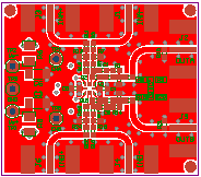 Figure 6-1 PCB Top Layers
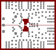 Figure 6-3 PCB Power Layer
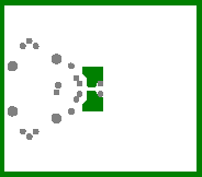 Figure 6-2 PCB Ground Layer
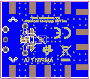 Figure 6-4 PCB Bottom Layers
SLOU562 September 2022
Figure 6-1 through Figure 6-4 show the PCB layers of the DRM-OPA-RUN-EVM board.
 Figure 6-1 PCB Top Layers
 Figure 6-3 PCB Power Layer
 Figure 6-2 PCB Ground Layer
 Figure 6-4 PCB Bottom Layers