SLUAAC9 March 2021 TPSM5D1806
5 TPSM5D1806 Dual-Output Frequency Considerations
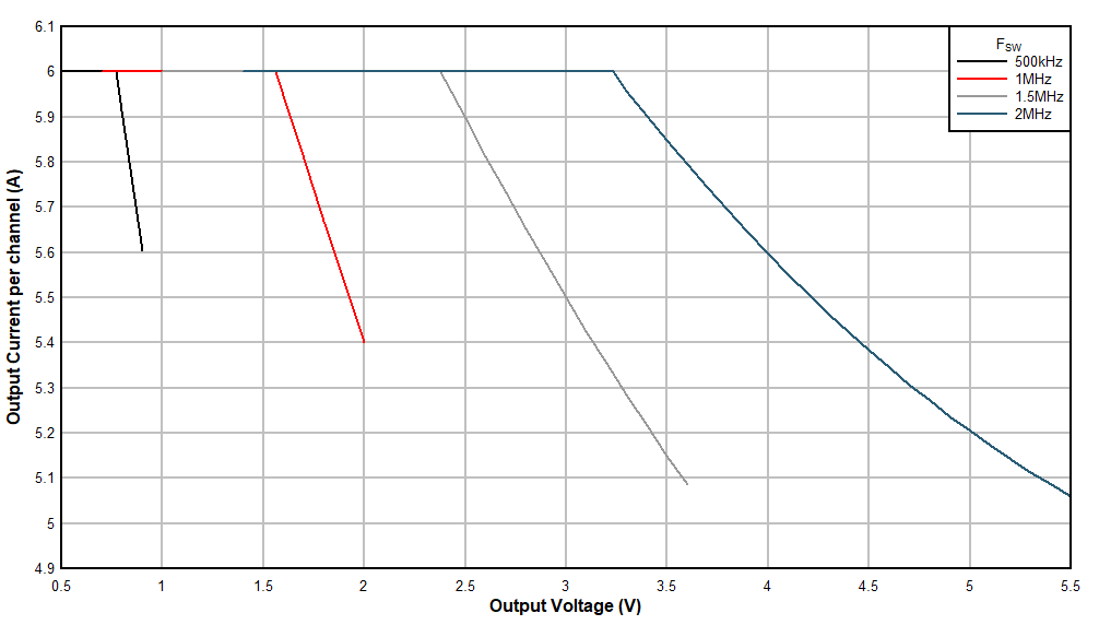
The frequency limitations due to minimum on-time, minimum off-time, and current limits all contribute to the operating boundaries summarized in Table 1-1. The same information is also displayed in graph form for Vin = 12 V in Figure 5-1.
The two channels of the TPSM5D1806 operate at the same selected frequency and 180° out of phase from one another in both dual-output and dual-phase operating modes. In dual-output mode, it is necessary to choose a common frequency at which the voltage and load current requirements of the two outputs can be simultaneously met.
Using Figure 5-1, the valid switching frequency options can be determined by finding the frequency curve(s) under which the two outputs’ voltage / current points reside. For example, for an application with VIN = 12 V and outputs of 1.8V at 6 A and 3.3V at 5A, either the 1.5-MHz or 2-MHz frequency settings can be used. As the figure also shows, not all combinations of output voltages and load currents may be combined in one TPSM5D1806. For example, there is no valid frequency to support VIN = 12V and outputs of 0.9 V at 6 A and 3.3 V at 6 A within one TPSM5D1806. While the 2-MHz setting would support the 3.3 V rail, the 0.9-V rail would violate minimum on-time with VIN = 12 V. Thus, some consideration has to be made when architecting the power tree for best utilization of the dual-output module channels.
 Figure 5-1 TPSM5D1806
Maximum Output Current (VIN = 12 V)