SLUAAD6 February 2021 TPS62866 , TPS62869
4 Simulation vs. Thermal Measurement
Simulation tools allow customer to evaluate their designs before manufacturing boards and assess the best implementation of their designs. Consequently, three versions of the PCB were simulated using Keysight’s Electro-thermal tool. The simulation setup considered is for Vin-3.3 V and Vout-0.9 V at 6 A load and ambient temperature (typically 25⁰C). The thermal images of the PCBs were then captured using FLIR T335 thermal imaging camera for the same test conditions. The results are as shown below.
 Figure 4-1 Simulation vs. Measurement for
E1
In the E1 version, the simulation and measurements resulted in a highest temperature of 97⁰C and 94.7⁰C respectively on the device.
 Figure 4-2 Simulation vs. Measurement for
E2
In the E2 version, the simulation and measurements resulted in a highest temperature of 107⁰C and 117⁰C respectively on the device.
 Figure 4-3 Simulation vs. Measurement for
E3
In the E3 version, the simulation and measurements resulted in a highest temperature of 97.7⁰C and 96⁰C respectively on the device.
It is then clear that the simulation results are not exactly similar to measurement results and this solely depends on the assumptions of the simulation models and the inaccuracy of real-time measurements. Nevertheless, from both the simulation and measurement, the hottest point of the PCB is on the device. It is seen that the lowest temperature is for E1 version and the highest for E2 version. The temperature of the device in E1 and E3 versions are very much comparable.
In addition to the reduction of the thermal resistance of the device, the optimization of the layout for thermals also can offer improvements in terms of efficiency. The use of thermal vias allows a better connection of the switching plane to inner layers of the design, by providing a low resistive path and consequently increases the switch node copper area. The fast swinging from the input voltage to ground at high frequency makes the switch node a critical thermal connection.
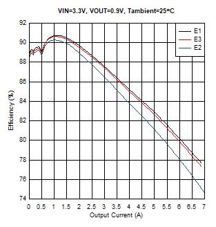
Table 4-1 shows the associated efficiency curves to the different layout implementations.
 Figure 4-4 Efficiency Comparison Between
Layouts
Figure 4-4 Efficiency Comparison Between
LayoutsThe efficiency curves comparison reflects that better efficiency results can be achieved by increasing copper area at the switching node. Thus, it is important to consider wide connection at the switch node.
| VIN=3.3 V/VOUT=0.9 V | E1 | E2 | E3 |
|---|---|---|---|
| Strategy | Performance optimized | Cost optimized | Performance and Cost |
| Max temperature at 6 A | 94.7°C | 117°C | 96°C |
| Peak efficiency | 90.75 % | 90.29 % | 90.66 % |