SLUAAJ6 april 2023 BQ25171-Q1 , BQ51013B-Q1
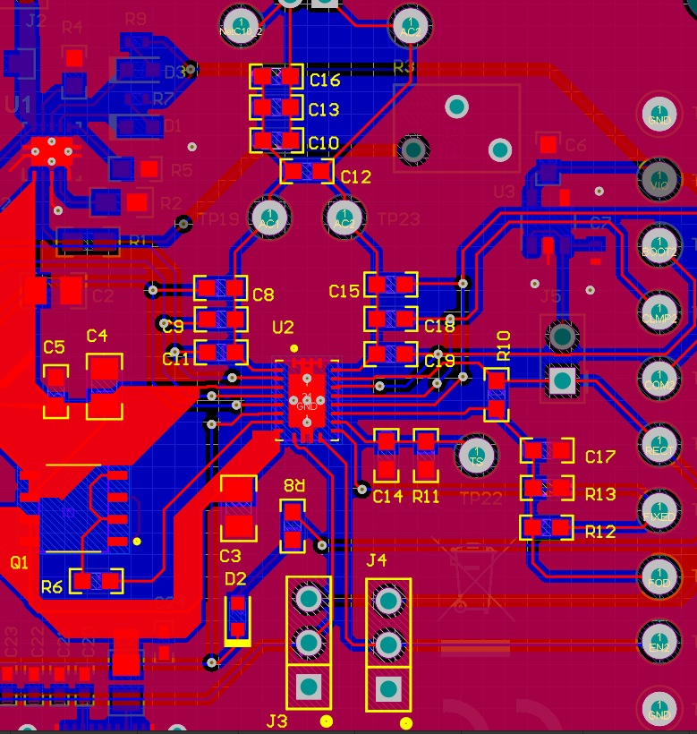
2.1 Wireless Receiver (BQ51013B-Q1)
- Keep the trace resistance as low as possible on AC1, AC2, and BAT.
- Detection and resonant capacitors must be as close to the device as possible.
- COMM, CLAMP, and BOOT capacitors must be placed as close to the device as possible.
- Via interconnect on PGND net is critical for appropriate signal integrity and proper thermal performance.
- High frequency bypass capacitors must be placed close to RECT and OUT pins.
- ILIM and FOD resistors are important signal paths and the loops in those paths to PGND must be minimized.
 Figure 2-1 Layout of BQ51013B-Q1