SLUAAL3 July 2022 UCC28C50-Q1 , UCC28C51-Q1 , UCC28C52-Q1 , UCC28C53-Q1 , UCC28C54-Q1 , UCC28C55-Q1 , UCC28C56H-Q1 , UCC28C56L-Q1 , UCC28C57H-Q1 , UCC28C57L-Q1 , UCC28C59-Q1
4 Current Filtering, Leading-Edge Blanking, and Slope Compensation
High-voltage and fast switching leads to a high dv/dt switching node, which generates a fair amount of noise. During PCB layout, the switching node must be kept away from quiet areas, such as the current sense circuitry, voltage feedback circuitry, and loop compensation components to reduce noise coupling.
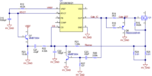
It’s common knowledge that each time the MOSFET turns on a spike appears on the current sense resistor for a very short time. This spike can cause the MOSFET to turn off early if precautions are not taken. The following figure shows several important sub-circuits required for reliable operation. First, and most important, R21 and C22 form a low pass filter between the (noisy) Rsense node and the CS pin. The low pass filter will attenuate most of the noise spike but too much filtering will delay the current information too. Second, Q6 and the components connected to its base are leading-edge blanking (LEB). This AC-coupled transistor pulls down on the CS voltage each time the MOSFET is turned on. The amount of leading-edge blanking is determined by C23, R26, and R27.
At duty cycles above 50%, current mode control in continuous conduction mode (CCM) is known to suffer from a subharmonic oscillation (instability) unless slope compensation is added. Since the backup power supply operates in wide input voltage range, the duty cycle can easily go above 50% and the converter runs into CCM at low input voltage condition. In Figure 4-1, R22 injects a small amount of voltage ramp to the CS pin. The voltage ramp for slope compensation is formed by passing the RT/CT voltage through an emitter-follower formed by Q7 and R23. The emitter follower buffers the RT/CT node so the switching frequency will not be altered. C21 ac-couples the output of the emitter follower to the CS pin (via R22). AC-coupling the slope compensation is preferred because it eliminates the addition of a DC bias at the CS pin if the slope compensation were directly coupled. The dc bias would effectively reduce the current limit threshold, requiring a smaller sense resistor, smaller current ramp, etc. Lastly, the value of R23 should be much higher than R21 to prevent attenuating the current signal at the CS pin.
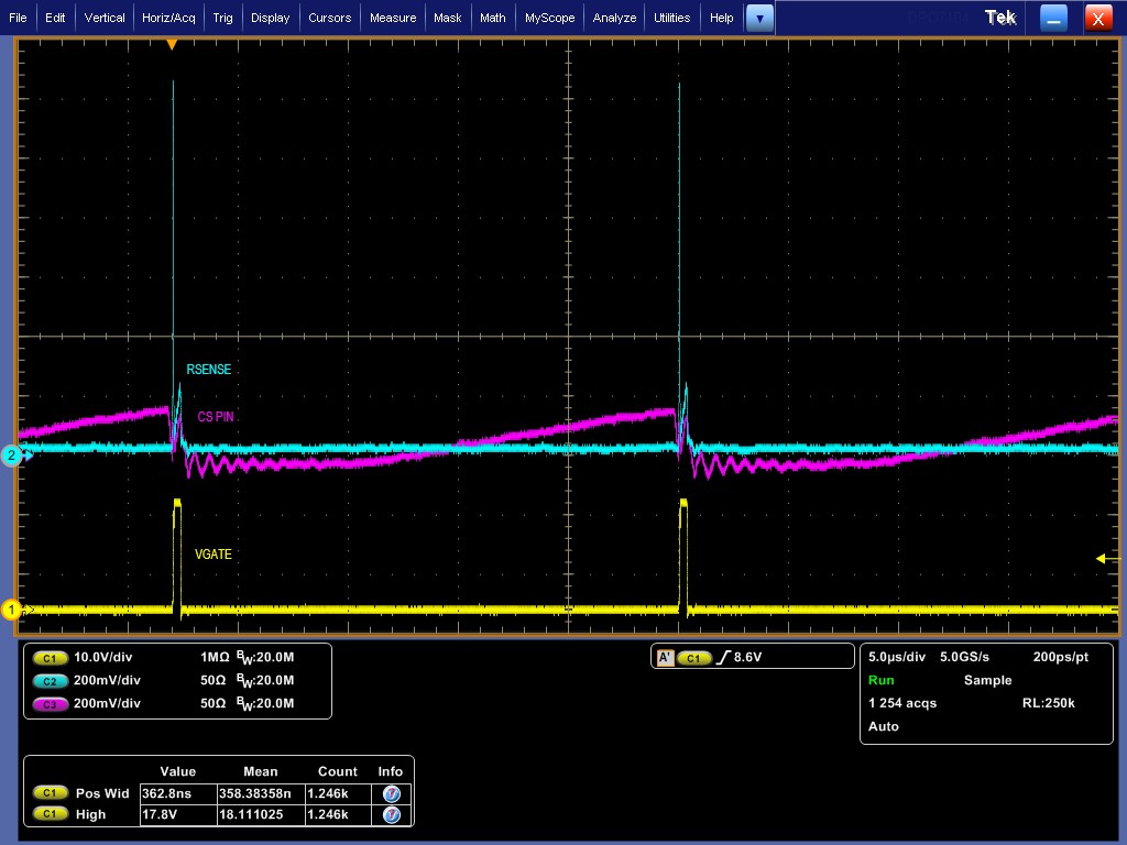
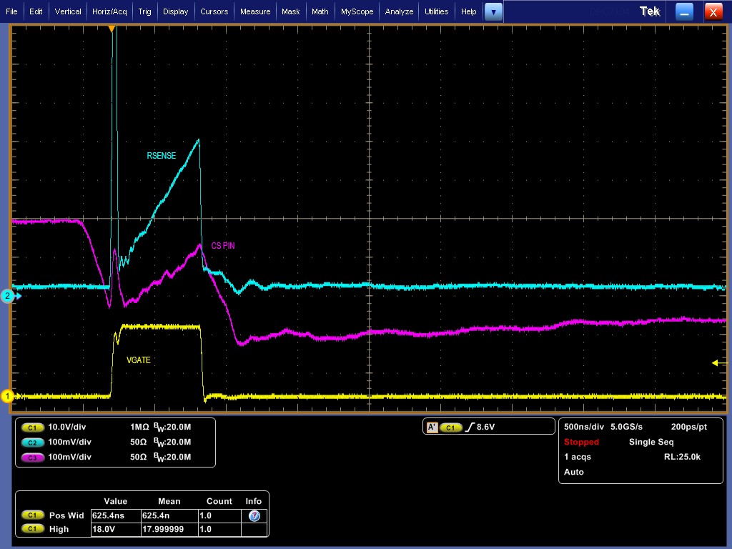
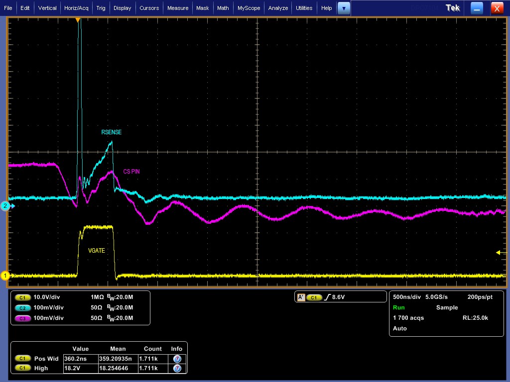
R23 (plus R22) form a resistor divider with R21. This resistor divider attenuates the current sense signal at the CS pin. If the current signal at the CS pin is too small the regulator will not be able to reliably produce small pulse width. Figure 4-2 to Figure 4-5 show differential measurements of the Rsense and CS pin voltages for two sets of values for R23.
 Figure 4-1 Current Filtering,
Leading-Edge Blanking, and Slope Compensation
Figure 4-1 Current Filtering,
Leading-Edge Blanking, and Slope CompensationIn the first pair of waveforms, R23 is 1 kΩ and C21 is 10nF. When the MOSFET turns on the CS signal starts from a value below 0 V (‒30 mV), has a much lower slope than Rsense, and peaks at only 140 mV when Rsense is at 400mV (35%). The regulator produces a “somewhat normal” pulse followed by an extremely narrow pulse. When the regulator operates in this manner the light load regulation is not very good. Pulse skipping occurs below 1 A load.
In the second pair of waveforms, R23 is increased to 15 kΩ and C21 to 2.2 µF. When the MOSFET turns on the CS signal starts from ~0V, has almost the same slope as Rsense, and peaks at 140 mV when Rsense is at 240 mV (58%). The regulator consistently produces pulse width of 358 ns and the light load regulation is much better. Pulse skipping does not occur until the load is less than 200 mA.

| Inconsistent gate pulse widths |

| Consistent gate pulse widths |

| CS signal starts below 0 V, slope of CS does not follow Rsense |

| CS signal starts at 0 V, slope of the CS follows Rsense |
Figure 4-6 shows load regulation for two sets of R23 and C21 values discussed. The light load regulation with 15 kΩ / 2.2 µF is significantly improved below 1-A load.