SLUP409B April 2022 – April 2024 TPS543320 , TPS543620 , TPS543820 , TPS62913 , TPS62916
- 1
- Abstract
- 1 Introduction
- 2 DC/DC Converters are Noisy
- 3 Power-Supply Output Voltage Ripple and Noise Degrade ADC Performance
- 4 Minimizing Low-Frequency Noise Requires Dedicated Low-Noise IC Technologies
- 5 Traditional Approaches to Reducing Ripple
- 6 Using Smaller Capacitors in Parallel
- 7 Larger Inductance
- 8 Adding a Feedthrough Capacitor
- 9 Adding a Ferrite Bead
- 10Layout Techniques
- 11Silicon Solutions
- 12Conclusions
10 Layout Techniques
Layout may be the most important part of the design when using a switching DC/DC regulator for many reasons, including the impact to output voltage ripple. A poorly constructed PCB layout can result in increased output ripple. The most important goal when creating a PCB layout for low ripple is to minimize the parasitic inductance. Adding inductance in series with the output capacitors will increase the ESL portion of the output ripple from the voltage divider from the switch node to the output. When designing for low output ripple, the ESL portion can often dominate the output ripple.
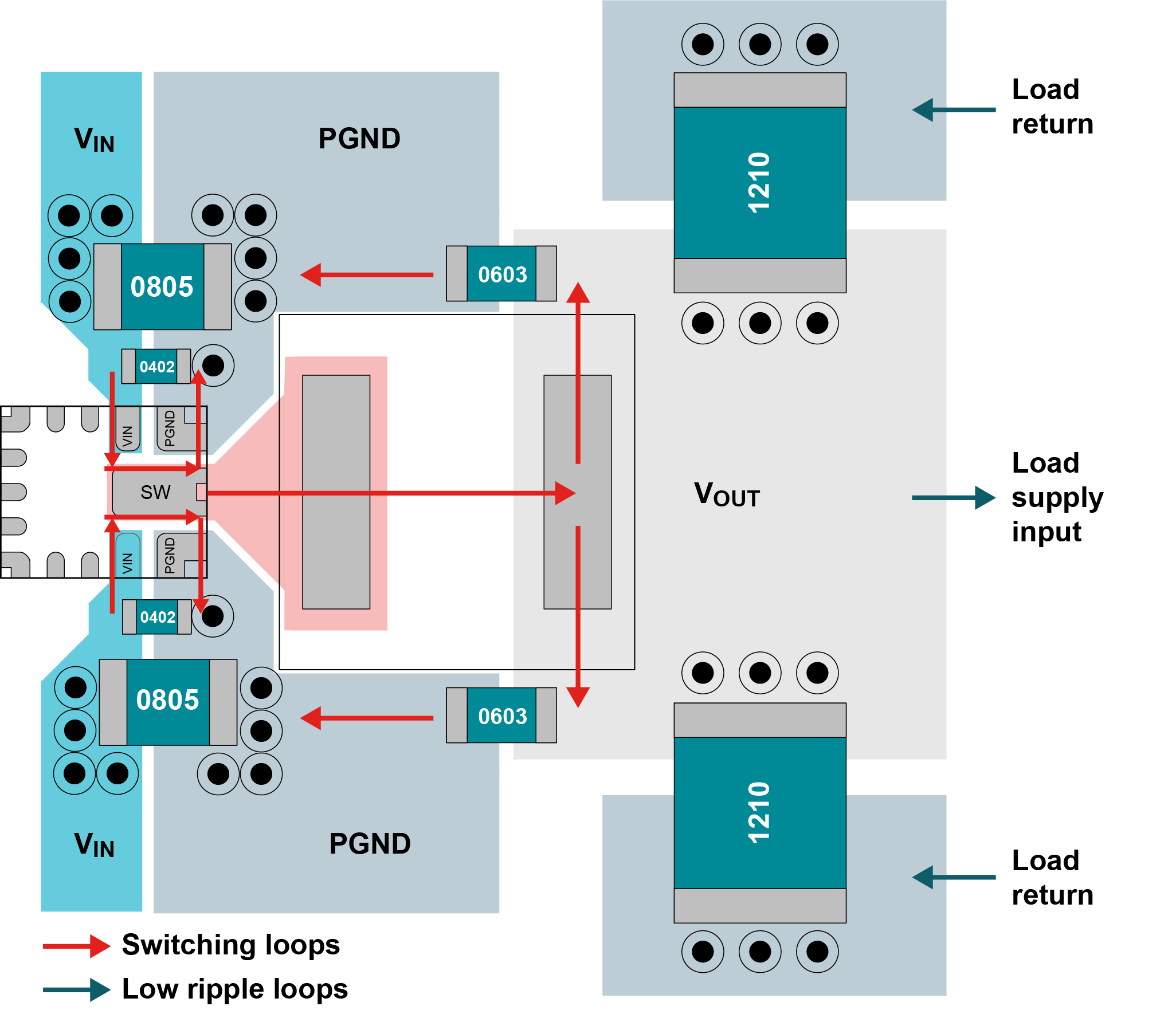
Figure 30 shows a simplified layout of the TPS543620. The TPS543620 has a “butterfly”-style pinout, with the input bypass capacitors placed on both sides of the device. The red arrows indicate the switching loops that require minimized parasitic inductance.
The green arrows indicate the output loops that require low ripple and noise.
 Figure 30 TPS543620 simplified
layout.
Figure 30 TPS543620 simplified
layout.To minimize the layout inductance (and as a result, the output ripple), use wide traces or planes for the input voltage (VIN), the power ground and the output voltage (VOUT). Avoid vias when routing these power signals, if possible. If other design constraints require vias, use multiple vias to minimize the parasitic inductance. To minimize the high-frequency noise caused by the rising and falling edges of the switching node, you’ll also need to minimize the input switching loop inductance, which will in turn minimize voltage stress on the power metal-oxide semiconductor field-effect transistors and reduce radiated noise. Avoid routing power rails that require low noise near high transient voltage (dv/dt) nets such as the switching node or the input switching loop of the regulator because noise can couple from the noisy nodes to low-noise power rails. For example, in Figure 30, the 1210 capacitors bypass the loop from the output of the regulator to the load return and connect to ground through an internal plane, away from the input switching loop.
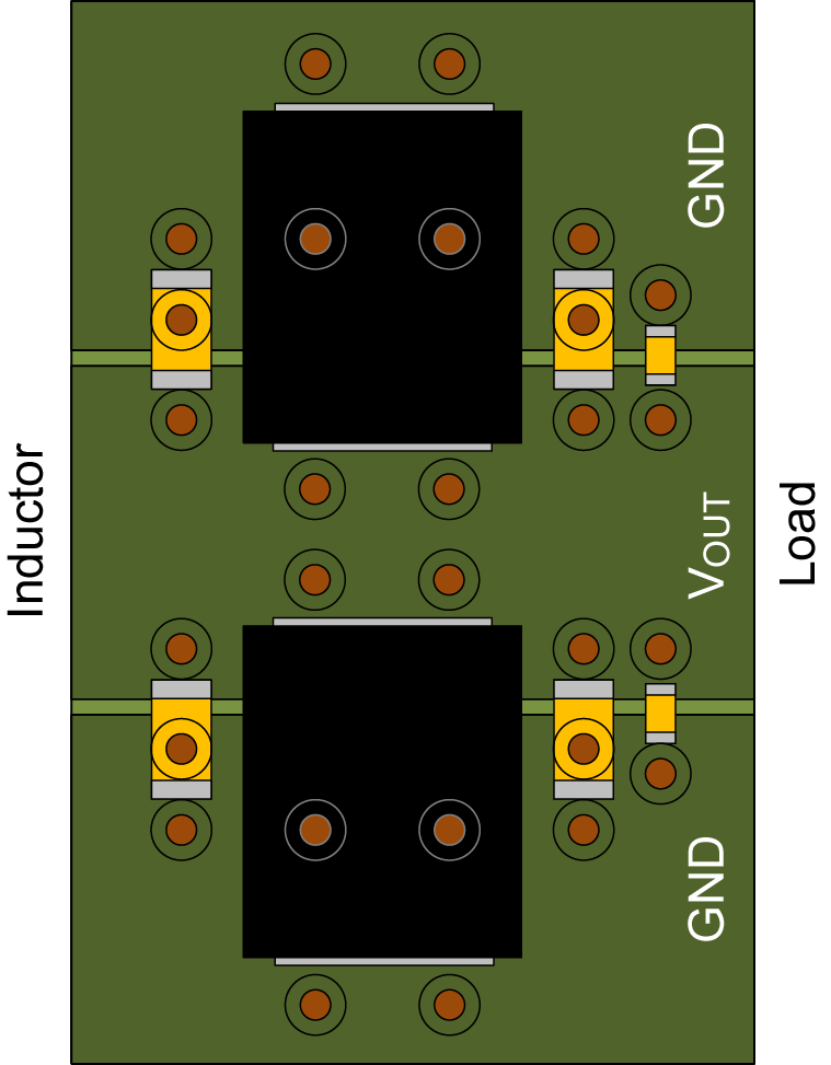
Figure 31 shows layout techniques to minimize parasitic inductance in the output capacitor layout between the regulator and the load. First, if possible, route VOUT between the output capacitor banks and ground.
Placing vias between the output capacitors’ terminals can reduce the loop area bypassed by the output capacitors, thus reducing the inductance. Figure 31 also shows also two sets of ground vias near each capacitor, with one set placed between the capacitor’s terminals.
 Figure 31 Output capacitor placement and
vias.
Figure 31 Output capacitor placement and
vias.When using multiple vias, space the vias to allow planes to fill between them, as shown in Figure 32. Placing vias close together creates a break in the other power planes they pass through on other layers. Spacing the vias further apart minimizes the inductance added by the other power planes.
 Figure 32 Vias spaced to allow planes to
fill between them.