SLUSAK2D August 2011 – April 2021 TPS53353
PRODUCTION DATA
- 1 Features
- 2 Applications
- 3 Description
- 4 Revision History
- 5 Pin Configuration and Functions
- 6 Specifications
-
7 Detailed Description
- 7.1 Overview
- 7.2 Functional Block Diagram
- 7.3
Feature Description
- 7.3.1 5-V LDO and VREG Start-Up
- 7.3.2 Adaptive On-Time D-CAP™ Control and Frequency Selection
- 7.3.3 Ramp Signal
- 7.3.4 Adaptive Zero Crossing
- 7.3.5 Power-Good
- 7.3.6 Current Sense, Overcurrent and Short Circuit Protection
- 7.3.7 Overvoltage and Undervoltage Protection
- 7.3.8 UVLO Protection
- 7.3.9 Thermal Shutdown
- 7.4 Device Functional Modes
- 8 Application and Implementation
- 9 Power Supply Recommendations
- 10Layout
- 11Device and Documentation Support
7.3.2 Adaptive On-Time D-CAP™ Control and Frequency Selection
The TPS53353 does not have a dedicated oscillator to determine switching frequency. However, the device operates with pseudo-constant frequency by feed-forwarding the input and output voltages into the on-time one-shot timer. The adaptive on-time control adjusts the on-time to be inversely proportional to the input voltage and proportional to the output voltage (tON ∝ VOUT/VIN).
This makes the switching frequency fairly constant in steady state conditions over a wide input voltage range. The switching frequency is selectable from eight preset values by a resistor connected between the RF pin and GND or between the RF pin and the VREG pin as shown in Table 7-1. (Maintaining open resistance sets the switching frequency to 500 kHz.)
| RESISTOR (RRF) CONNECTIONS | SWITCHING FREQUENCY (fSW) (kHz) | |
|---|---|---|
| VALUE (kΩ) | CONNECT TO | |
| 0 | GND | 250 |
| 187 | GND | 300 |
| 619 | GND | 400 |
| OPEN | n/a | 500 |
| 866 | VREG | 650 |
| 309 | VREG | 750 |
| 124 | VREG | 850 |
| 0 | VREG | 970 |
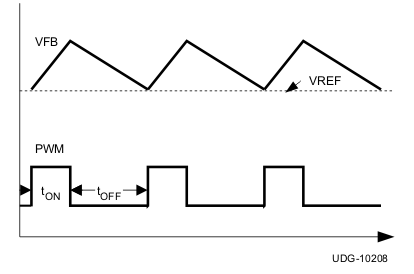
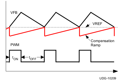
The off-time is modulated by a PWM comparator. The VFB node voltage (the mid-point of resistor divider) is compared to the internal 0.6-V reference voltage added with a ramp signal. When both signals match, the PWM comparator asserts a set signal to terminate the off time (turn off the low-side MOSFET and turn on high-side MOSFET). The set signal is valid if the inductor current level is below the OCP threshold, otherwise the off time is extended until the current level falls below the threshold.
Figure 7-2 and Figure 7-3 show two on-time control schemes.
 Figure 7-2 On-Time Control Without Ramp Compensation
 Figure 7-3 On-Time Control With Ramp Compensation