SLUSCA8A February 2016 – February 2016 UCC28704
PRODUCTION DATA.
- 1 Features
- 2 Applications
- 3 Description
- 4 Revision History
- 5 Pin Configuration and Functions
- 6 Specifications
-
7 Detailed Description
- 7.1 Overview
- 7.2 Functional Block Diagram
- 7.3
Feature Description
- 7.3.1 Detailed Pin Description
- 7.3.2 Primary-Side Regulation (PSR)
- 7.3.3 Primary-Side Constant Voltage (CV) Regulation
- 7.3.4 Primary-Side Constant Current (CC) Regulation
- 7.3.5 Valley-Switching and Valley-Skipping
- 7.3.6 Start-Up Operation
- 7.3.7 Fault Protection
- 7.3.8 Constant Current Under-Voltage Protection
- 7.3.9 Load Transient Response
- 7.4 Device Functional Modes
-
8 Applications and Implementation
- 8.1 Application Information
- 8.2
Typical Application
- 8.2.1 Design Requirements
- 8.2.2
Detailed Design Procedure
- 8.2.2.1 VDD Capacitance, CDD
- 8.2.2.2 VDD Start-Up Resistance, RSTR
- 8.2.2.3 Input Bulk Capacitance and Minimum Bulk Voltage
- 8.2.2.4 Transformer Turns Ratio, Inductance, Primary-Peak Current
- 8.2.2.5 Transformer Parameter Verification
- 8.2.2.6 VS Resistor Divider, Line Compensation, and NTC
- 8.2.2.7 Standby Power Estimate
- 8.2.2.8 Output Capacitance
- 8.2.2.9 Design Considerations in Using with Synchronous Rectifiers
- 8.2.3 Application Curves
- 8.3 Do's and Don'ts
- 9 Power Supply Recommendations
- 10Layout
-
11Device and Documentation Support
- 11.1
Device Support
- 11.1.1
Device Nomenclature
- 11.1.1.1 Capacitance Terms in Farads
- 11.1.1.2 Duty Cycle Terms
- 11.1.1.3 Frequency Terms in Hertz
- 11.1.1.4 Current Terms in Amperes
- 11.1.1.5 Current and Voltage Scaling Terms
- 11.1.1.6 Transformer Terms
- 11.1.1.7 Power Terms in Watts
- 11.1.1.8 Resistance Terms in Ω
- 11.1.1.9 Timing Terms in Seconds
- 11.1.1.10 Voltage Terms in Volts
- 11.1.1.11 AC Voltage Terms in VRMS
- 11.1.1.12 Efficiency Terms
- 11.1.1
Device Nomenclature
- 11.2 Documentation Support
- 11.3 Community Resources
- 11.4 Trademarks
- 11.5 Electrostatic Discharge Caution
- 11.6 Glossary
- 11.1
Device Support
- 12Mechanical, Packaging, and Orderable Information
7 Detailed Description
7.1 Overview
The UCC28704 flyback power supply controller provides accurate constant voltage and constant current regulation with primary-side feedback control. It also eliminates the need for opto-coupler feedback circuits. The controller optimizes the modulation scheme and the device's power management to boost power conversion efficiency, lower power dissipation at no-load and light load. Frequency dithering reduces the EMI peak energy at the fundamental switching frequency and harmonics. Features include fixed cable compensation and constant current output under-voltage shutdown, or CCUV, to protect USB terminals from getting over-heated or burn-out condition during soft-short circuit fault.
The controller operates in discontinuous conduction mode with valley switching to minimize switching losses. A combination of frequency modulation and primary peak current modulation to provide high power conversion efficiency across the load range. Accurate voltage and constant current regulation, fast dynamic response, and fault protection are achieved with primary-side control. A complete charger solution can be realized with a straightforward design process, low cost and low component count.
In UCC28704, as compared to UCC28700/1/2/3, features such as constant current under voltage protection and enhanced load transient schemes have been added. Also, in UCC28704, the demagnetizing ratio has been extended to 0.475 along with an increased AM ratio of 4:1. The maximum frequency of the controller is set at 85 kHz and the AM region switching frequency is optimally set at 25 kHz to have better trade-offs between no-load standby power consumption and load transient response. UCC28704 also incorporates schemes to have better noise rejection at the output voltage sense (VS pin) allowing for improved output voltage ripple reduction.
7.2 Functional Block Diagram
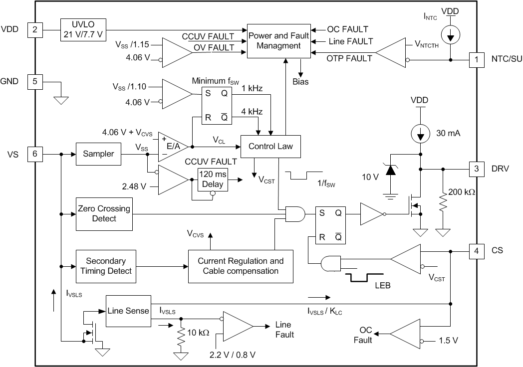
7.3 Feature Description
7.3.1 Detailed Pin Description
7.3.1.1 VDD (Device Bias Voltage Supply)
The VDD pin is typically powered from a rectified auxiliary transformer winding, the same winding that is used to capture the output voltage level. A bypass capacitor, with minimum value 0.047 μF, on the VDD pin is used for initially biasing the device to start-up along with a resistive or active source of start-up charging current. UVLO start / stop levels of 21 V / 7.7 V accommodate lower values of VDD capacitance that in turns keeps the start-up current low, which for resistive start-up has an impact on both stand-by power and power-on delay. A high, 35-V, maximum operating level on VDD alleviates concerns with leakage energy charging of VDD and gives added flexibility to when varying power supply output voltage must be supported.
7.3.1.2 GND (Ground)
This is an external return pin, and provides the reference point for both external signal and the gate drive of the device. The VDD bypass capacitor should be placed close to this pin. Critical component GND connections from the VS, CS and NTC pins should have dedicated and short paths to this pin.
7.3.1.3 VS (Voltage-Sense)
The VS pin is connected to a resistor divider from the auxiliary winding to ground. The output-voltage feedback information is sampled at the end of the transformer secondary current demagnetization time to provide an accurate representation of the output voltage. Timing information to achieve valley-switching and to control the duty cycle of the secondary transformer current is determined by the waveform on the VS pin. The VS input is a critical signal and will generally be with relatively high impedance. To avoid unpredictable behavior avoid placing a filter capacitor on this pin and keep the total PCB area tied to VS at a minimum.
The VS pin also senses the bulk capacitor input voltage to provide for ac-input run and stop thresholds, and to compensate the current-sense threshold across the AC-input range. This information is sensed by monitoring the current pulled out of the VS pin during the MOSFET on-time. During this time the voltage on the VS pin is clamped to about 250mV below GND. As a result, the current out of the pin is determined by the upper VS divider resistor, the auxiliary to primary turns-ratio and the bulk input voltage level. For the AC-input run/stop function, the run threshold on VS is IVSL(run) (typical 220 µA) and the stop threshold is IVSL(stop) (typical 80 µA). The values for the auxiliary voltage divider upper-resistor RS1 and lower-resistor RS2 can be determined by the equations below.

where
- NPA is the transformer primary-to-auxiliary turns ratio,
- VIN(run) is the AC rms voltage to enable turn-on of the flyback converter (run),
- VBULK(run) is the DC bulk voltage to enable turn-on of the flyback converter (run),
- IVSL(run) is the run-threshold for the current pulled out of the VS pin during the primary MOSFET on-time. (see the Electrical Characteristics table).

where
- VOCV is the converter regulated output voltage,
- VF is the output rectifier forward voltage drop at near-zero current,
- NAS is the transformer auxiliary to secondary turns ratio,
- RS1 is the VS divider high-side resistance,
- VVSR is the CV regulating level at the VS input (see the Electrical Characteristics table).
This pin is also used to sense the output constant current under voltage (CCUV) level, used to shut down the converter in the case of a soft-short circuit at its output. Refer to Constant Current Under-Voltage Protection for further information.
7.3.1.4 DRV (Gate Drive)
The DRV pin is connected to the MOSFET gate pin, usually through a series resistor. The DRV provides a gate drive signal which is clamped to 10.5-V internally. During turn-on the driver applies a typical 30-mA current source out of the DRV pin. When the DRV voltage rises to above 9 V the output current is reduced to about 100 µA. This current brings the DRV voltage to the 10.5-V clamp level, or to VDD, whichever is less. The 30-mA current provides adequate turn-on speed while automatically limiting noise generated at turn-on by the MOSFET drain dv/dt and by the leading edge turn-on current spike. The gate drive turn-off current is internally limited to about 400 mA when DRV is above about 4 V. At lower DRV voltages the current will reduce, eventually being limited by the low-side on resistance, RDS(on). The drain turn-on and turn-off dv/dt can be further impacted by adding external resistor in series with DRV pin. The drain current resonances can be damped with a small series gate resistor, generally less than a 1 Ω.
7.3.1.5 CS (Current Sense)
The current sense pin is connected through a series resistor (RLC) to the current-sense resistor (RCS). The controller varies the internal current sense threshold between 0.188 V and 0.75 V, setting a corresponding control range for the peak-primary winding current to a 4-to-1 range. The series resistor RLC provides an input voltage feed-forward function. The voltage drop across this resistor reduces primary-side peak current as the line voltage increases, compensating for the increased di/dt and delays in the MOSFET turn-off. There is an internal leading-edge blanking time of 255 ns to eliminate sensitivity to the MOSFET turn-on leading edge current spike. If additional blanking time is needed, a small bypass capacitor, up to 30 pF, can be placed on between CS pin and GND pin. The value of RCS is determined by the target output current in constant current (CC) regulation. The values of RCS and RLC can be determined by the equations below. The term ηXFMR is intended to account for the energy stored in the transformer but not delivered to the secondary. This includes transformer core and copper losses, bias power, and primary leakage inductance losses.
Example: With a transformer core and copper losses of 3%, leakage inductance caused power losses 2%, and bias power to output power ratio of 0.5%. The transformer power transfer efficiency is estimated as ηXFMR = 100% - 3% - 2% - 0.5% = 94.5%

where
- VCCR is a current regulation constant (see the Electrical Characteristics table),
- NPS is the transformer primary-to-secondary turns ratio (a typical turns-ratio of 12 to 15 is recommended for 5-V output),
- IOCC is the target output current in constant-current regulation,
- ηXFMR is the transformer efficiency.

where
- RS1 is the VS pin high-side resistor value,
- RCS is the current-sense resistor value,
- tD is the current-sense delay (typical 50 ns) plus MOSFET turn-off delay,
- tGATE_OFF is the primary-side main MOSFET turn-off time,
- NPA is the transformer primary-to-auxiliary turns-ratio,
- LP is the transformer primary inductance,
- KLC is a current-scaling constant (see the Electrical Characteristics table).
7.3.1.6 NTC/SU (NTC Thermistor Shutdown and External Start Up Control)
The UCC28704 uses an external NTC resistor tied to the NTC/SU pin to program a thermal shutdown temperature for the power supply. The NTC/SU shutdown threshold is 0.95 V with an internal 105-µA current source which results in a 9.05-kΩ thermistor shutdown threshold. A small capacitor with value not greater than 100 pF can be used on this pin for any noise reduction purposes. The capacitor with its value greater than 100 pF can cause a false over-temperature protection response. The NTC/SU pin should be left floating if not used.
The NTC/SU pin can be used to control an external depletion-mode FET to enable active high-voltage start up, Refer to Initial Power-On with A Depletion-Mode FET for more detail.
7.3.2 Primary-Side Regulation (PSR)
Figure 12 illustrates a simplified flyback convertor with the main voltage regulation blocks of the device shown. The power train operation is the same as any DCM flyback circuit but accurate output voltage and current sensing is the key to primary-side control.
 Figure 12. Simplified Flyback Convertor
 (with the Main Voltage Regulation Blocks)
In primary-side control, the output voltage is sensed on the auxiliary winding during the transfer of transformer energy to the secondary. As shown in Figure 13 during this time, the auxiliary winding voltage has a down slope representing a decreasing total rectifier forward voltage drop VF and resistance voltage drop (ISRS) as the secondary current decreases to zero. To achieve an accurate representation of the secondary output voltage on the auxiliary winding, the discriminator reliably blocks the leakage inductance reset and ringing, continuously samples the auxiliary voltage during the down slope after the ringing is diminished, and captures the error signal at the time the secondary winding reaches zero current. The internal reference on VS is 4.06 V; the resistor divider is selected as outlined in the VS pin description.
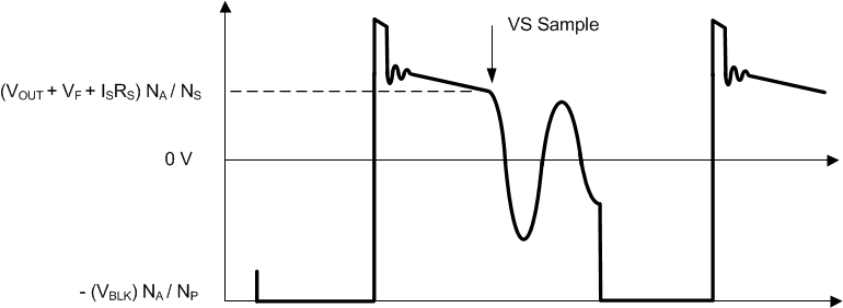 Figure 13. Auxiliary Winding Voltage
The UCC28704 VS signal sampler includes signal discrimination methods to ensure an accurate sample of the output voltage from the auxiliary winding. There are however critical details of the auxiliary winding signal to ensure reliable operation, specifically the reset time of the leakage inductance and the duration of any subsequent leakage inductance ring. Refer to Figure 14 for a detailed illustration of waveform criteria to ensure a reliable sample on the VS pin. The first detail to examine is the duration of the leakage inductance reset pedestal, TLK_RESET in Figure 14. Since this can mimic the waveform of the secondary current decay, followed by a sharp downslope, it is important to keep the leakage reset time less than 750 ns for IPRI minimum, and less than 3.0 µs for IPRI maximum. The second detail is the amplitude of ringing on the VAUX waveform following tLK_RESET. The peak-to-peak voltage at the VS pin should be less than approximately 250 mVp-p at least 250 ns before the end of the demagnetization time, tDMAG. If there is a concern with excessive ringing, it usually occurs during light or no load conditions, when tDMAG is at the minimum, tDMAG(min). The tolerable ripple on VS is scaled up to the auxiliary winding voltage by RS1 and RS2, and is equal to 250 mV × (RS1+RS2) / RS2. The snubber designs can be designed to allow the ripple voltage to meeting these requirements.
As mentioned in Device Functional Modes, when IPP < IPP(max), the device operation enters a “Wait” state during each switching cycle of its non-switching portion as shown in Figure 14. In the Wait state, the device bias current changes to IWAIT (typical 70 µA) from IRUN (typical 2.3 mA), reducing its bias power to help boost efficiency at light load and to reduce standby load power.
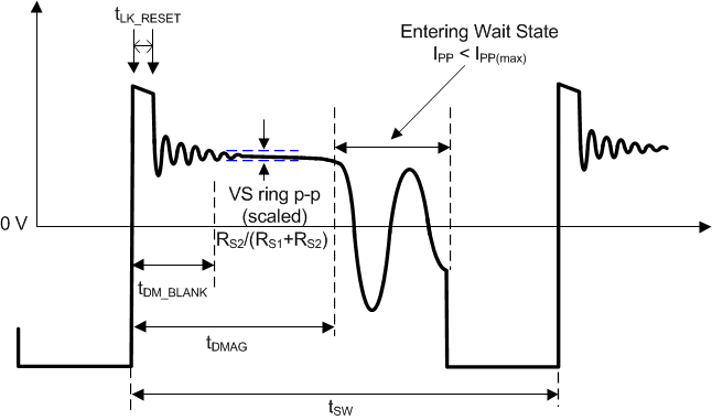 Figure 14. Auxiliary Waveform Details
7.3.3 Primary-Side Constant Voltage (CV) Regulation
During voltage regulation (CV mode), the controller operates in frequency modulation mode and peak current amplitude modulation mode as illustrated in Figure 15 below. The UCC28704 incorporates internal voltage-loop compensation circuits so that external compensation is not necessary, provided that the value of COUT is high enough. The following equation determines a minimum value of COUT necessary to maintain a phase margin of about 40 degrees over the full-load range,

The internal operating frequency limits of the device are fSW(max) and fSW(min), typically 85 kHz and 1 kHz, respectively. The choice of transformer primary inductance and primary-peak current sets the maximum operating frequency of the converter, which must be equal to or lower than fSW(max). Conversely, the choice of maximum target operating frequency and primary-peak current determines the transformer primary-inductance value. The actual minimum switching frequency for any particular converter depends on several factors, including minimum loading level, leakage inductance losses, switch-node capacitance losses, other switching and conduction losses, and bias-supply requirements. In any case, the minimum steady-state frequency of the converter must always exceed fSW(min) or the output voltage may rise to the over-voltage protection level (OVP) and the controller responds as described in Fault Protection.
To achieve a regulated output voltage in the CV mode operation, energy balance has to be maintained. As the UCC28704 has a minimum switching frequency typical 1 kHz, together with the energy per switching cycle determined by converter parameters, such as the transformer primary inductance Lp and the selected RCS resistor, the converter has a minimum input power. A proper pre-load needs to be selected to ensure that this minimum energy is balanced during the no-load condition. The selection of the line compensation resistor value (RLC) connected to the CS pin can impact the energy per switching cycle based on low-line and high-line conditions. Typical Application section provides a design example to show how to implement these considerations.
In the CV mode operation, the cable compensation is in effect. The cable compensation is to adjust the output voltage at board-end to be higher than the no-load setup point, noted as VOCV, then to compensate the voltage drop due to the cable resistance through which the load current IO is flowing. The UCC28704 cable compensation is fixed at 6% of VOCV at full load, and the board-end output voltage is described by Equation 6:

Due to the cable compensation, the output voltage at board-end is seen higher than VOCV with a positive slope when load current IO> 0. The output voltage at the cable's end can be flat, upturned, or downturned, depending on the cable total resistance in use. Primary-Side Constant Current (CC) Regulation has more descriptions on the cable compensation.
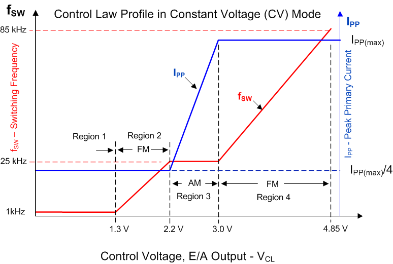 Figure 15. Frequency and Amplitude Modulation Modes
 (during CV mode)
In CV mode operation, the control consists of four regions, namely, region 1 through 4. The device internal error op-amp output VCL sets a particular region operation. Refer to Figure 12 for VCL. The steady-state control-law voltage, VCL, ranges between 1.3 V to 4.85 V. Heavy load operation is usually in region 4 where frequency modulation to output regulation is used and primary-peak current is controlled at its maximum. Region 3 is usually for medium-load range typically from 10% load and above. In this region switching frequency is fixed at nominal 25 kHz along with primary-peak current varying from 25% to 100% of its maximum. A low operating frequency range (region 2) is for lighter loads to achieve stable regulation at low frequencies. In region 2, peak-primary current is always maintained at IPP(max)/4 in the lower frequency level. Transitions between levels are automatically accomplished by the controller depending on the internal control-law voltage, VCL. During a load transient condition when VCL > 4.85 V, the device operates in constant current mode. When load is in step-down transient demanding frequency lower than 4 kHz, first, the device stays at 4 kHz for up to 500 ms, or the output voltage reaches about 10% over the VOCV within 500 ms, then the device adjusts the switching frequency to be lower than 4 kHz as needed. More details can be found in Load Transient Response.
7.3.4 Primary-Side Constant Current (CC) Regulation
Timing information at the VS pin and current information at the CS pin allow accurate regulation of the secondary average current. The control law dictates that as power is increased in CV regulation and approaching CC regulation the primary-peak current is at IPP(max). Referring to Figure 16 below, the primary peak current (IPP), turns-ratio (NS/NP), secondary demagnetization time (tDMAG), and switching period (tSW) determine the secondary average output current. Ignoring leakage inductance effects, the average output current is given by Equation 7. By regulating the secondary rectifier conduction duty cycle, the output average current is constant for given IPP and transformer turns-ratio. When the load increases, the secondary-side rectifier conduction duty cycle keep increasing. Once it reaches preset value of 0.475, the converter switching frequency is then reduced to maintain 0.475 secondary-side duty cycle. Therefore, the output current is kept constant. Because the current is kept constant, the increasing load results in lower output voltage. Converter can shut down in this condition if the output voltage drops below CCUV protection level, or UCC28704 VDD drops below its UVLO turn-off threshold.
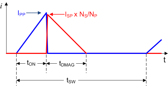 Figure 16. Transformer Currents

As shown in Figure 17 below, CV mode operation is from IO = 0 to IOCC; at IO = IOCC, the operation enters CC mode and VO starts to drop as the load resistance becomes further lower while IO is maintained at IOCC until Vo reaches the CCUV threshold. Details of the CCUV operation are given in Constant Current Under-Voltage Protection. Figure 17 shows the output at board-end and at cable-end. The cable compensation nominally compensates 300 mV for a 5V-output at the IOCC level.
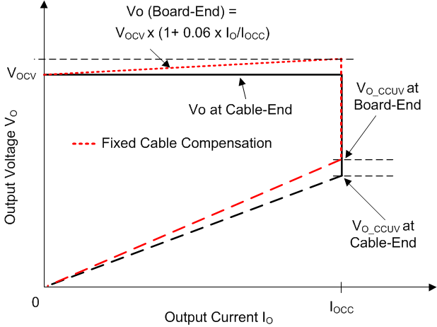 Figure 17. Typical Target Output V-I Characteristic
7.3.5 Valley-Switching and Valley-Skipping
The UCC28704 utilizes valley switching to reduce switching losses in the MOSFET, reduce induced-EMI, and minimize the turn-on current spike at the sense resistor. The controller operates in valley-switching in all load conditions unless the VDS ringing diminished.
Referring to Figure 18 below, the UCC28704 operates in a valley-skipping mode in most load conditions to maintain an accurate voltage or current regulation point and still switch on the lowest available VDS voltage.
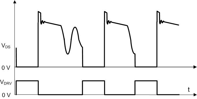 Figure 18. Valley-Skipping Mode
The UCC28704 forces a controlled minimum switching period corresponding to the power supply operating frequency. In each switching cycle, after the minimum period is expired, the UCC28704 looks for the next resonant valley on the auxiliary winding. The controller initiates a new power cycle at this valley point which corresponds to a reduced voltage level on the power MOSFET. If at the point in time when the minimum period expires ringing on the transformer winding has decayed such that no further resonant valleys can be detected a new power cycle is initiated following a fixed time, tZTO.
7.3.6 Start-Up Operation
Upon application of input voltage to the converter, the start up resistance connected to VDD from the bulk capacitor voltage (VBULK) charges the VDD capacitor. During charging of the VDD capacitor, the device supply current is less than 1.5 µA. When VDD reaches the 21-V UVLO turn-on threshold, the controller is enabled and the converter starts switching. The peak-primary currents with initial three cycles are limited to IPP(min). This allows sensing any initial input or output faults with minimal power delivery. When confirmed that the input voltage is above the programmed converter turn-on voltage and with no faults detected, the start-up process proceeds and normal power conversion follows. The converter remains in discontinuous conduction mode operation during charging of the output capacitor(s), maintaining a constant output current until the output voltage is in regulation.
Initial power-on to the UCC28704 device is achieved by one of the two approaches that are described in Initial Power-On with a Start-Up Resistor and Initial Power-On with A Depletion-Mode FET.
7.3.6.1 Initial Power-On with a Start-Up Resistor
A common used initial power-on approach for UCC28704 is to use a start-up resistor, RSTR, to tie VDD to VBLK, as show in Figure 19. With this approach, the VDD pin is connected to a bypass capacitor to ground and a start-up resistance to the input bulk capacitor (+) terminal. The VDD turn-on UVLO threshold is 21 V (VVDD(on))and turn-off UVLO threshold is 7.7 V (VVDD(off)), with an available operating range up to 35 V. The USB charging practice requires the output current to operate in constant-current mode from 5 V to typical about 3 V; this is easily achieved with a nominal VDD of approximately 15 V. The additional VDD headroom up to 35 V allows for VDD to rise due to the leakage energy delivered to the VDD capacitor in high-load conditions. Also, the wide VDD range provides the advantage of selecting a relatively small VDD capacitor and high-value start-up resistance to minimize no-load stand-by power loss in the start-up resistor.
The RSTR value has effect to power-on delay time and no-load standby power losses. Both are usually part of the design specifications. Increase RSTR reduces standby power losses while increases power-on delay time. A typical range of RSTR is from 10 MΩ to 15 MΩ as initial design start point for off-line AC-to-DC adapters where power-on delay time usually requires less than two seconds. Due to the limited voltage rating, RSTR is normally implemented by two or three resistors in series.
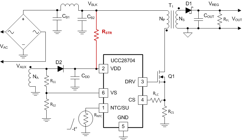 Figure 19. Power-On with Start-Up Resistor
7.3.6.2 Initial Power-On with A Depletion-Mode FET
The UCC28704 NTC/SU pin can control an external depletion-mode FET to provide more efficient start-up. This provides a fast start-up time with eliminating the loss associated with the start-up circuit. Therefore, the standby power at no load can be minimized. This gives an alternative method to power on the device initially. As shown in Figure 20, the depletion mode FET HV start-up circuit consists of QST1, QST2, CST, RILIM, and RST1 to RST3.
Before VDD reaches VVDD(on), NTC/SU stays low, QST1 turns on, which enables the quick charge of CDD thereby achieving a shorter power-on delay time. After VDD ≥ VVDD(on), NTC/SU starts sourcing 105 µA to turn on QST2 then turns off QST1. This stops QST1 providing current to UCC28704 and minimizes the loss in the start-up circuit. In normal operation when IPP < IPP(max), the device enters wait state in each switching cycle, see Figure 14 for wait state time. During wait state, NTC/SU stops sourcing 105 µA; which turns off QST2 and can potentially cause QST1 to turn on. Hence CST is added to ensure that QST1 is off even during wait state. For reference, RST1 = RST2 = 2 MΩ, RST3 = 100 kΩ, CST = 1 nF, RILIM = 365 kΩ, as an example. To select a depletion-mode FET for QST1, BSS126 or similar can be an option.
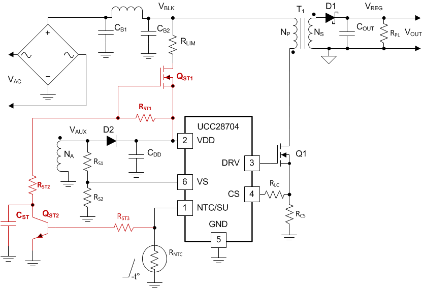 Figure 20. Power-On with a Depletion-Mode FET
7.3.7 Fault Protection
There is comprehensive fault protection incorporated into the UCC28704. Protection functions include:
- Output Over-Voltage
- Input Under-Voltage
- Primary Over-Current Fault
- CS Pin Open Fault
- CS Pin Short-to-GND Fault
- VS Pin Fault
- External NTC Over-Temperature
- Device Internal Over-Temperature
- Constant Current Under Voltage Output Shutdown (CCUV) for Soft-Short Protection
Output Over-Voltage: The output over-voltage function is determined by the voltage feedback on the VS pin. If the voltage sample on VS exceeds 4.67 V, 115% of the nominal regulating level, for three consecutive switching cycles an OV fault is asserted. Once asserted the device stops switching, initiating a UVLO reset and re-start fault cycle. During the fault, the VDD bias current remains at the run current level, discharging the VDD pin to the UVLO turn-off threshold, VVDD(off). After that, the device returns to the start state, VDD now charging to VVDD(on) where switching is initiated. The UVLO sequence repeats as long as the fault condition persists.
Input Under-Voltage: The line input run and stop thresholds are determined by current information at the VS pin during the MOSFET on-time. While the VS pin is clamped close to GND during the MOSFET on-time, the current through RS1, out of the VS pin, is monitored to determine a sample of the bulk capacitor voltage. A wide separation of run and stop thresholds allows clean start-up and shut-down of the power supply with the line voltage. From the start state, the sensed VS current, IVSL, must exceed the run current threshold, IVSL(run) (typical 220 µA), within the first three cycles after switching starts as VDD reaches VVDD(on). If it does not, then switching stops and the UVLO reset and re-start fault cycle is initiated. Once running, IVSL must drop below the stop level, IVSL(stop) (typically 80 µA), for three consecutive cycles to initiate the fault response.
Primary Over-Current: The UCC28704 always operates with cycle-by-cycle primary-peak current control. The normal operating range of the CS pin is 0.75 V to 0.188 V. If the voltage on CS exceeds the 1.5-V over-current level, any time after the internal leading edge blanking time and before the end of the transformer demagnetization, for three consecutive cycles the device shuts down and the UVLO reset and re-start fault cycle begins.
CS Pin Open: The CS pin has a 2-µA minimum pull-up that brings the CS pin above the 1.5-V OC fault level if the CS pin is open. This causes the primary over-current fault after three cycles.
CS Pin Short to GND: On the first, and only the first cycle at start-up, the device checks to verify that the VCST(min) threshold is reached at the CS pin within 4 µs of DRV going high. If the CS voltage fails to reach this level then the device terminates the current cycle and immediately enters the UVLO reset and re-start fault sequence.
VS Pin: Protection is included in the event of component failures on the VS pin. If the high-side VS divider resistor opens the controller stops switching. VDD collapses to its VVDD(off) threshold, a start-up attempt follows with a single DRV on-time when VDD reaches VVDD(on). The UVLO cycle will repeat. If the low-side VS divider resistor is open then an output over-voltage fault occurs.
NTC Over-Temperature: UCC28704 uses the NTC/SU pin to program thermal shutdown threshold with an external NTC thermistor on this pin. The NTC shutdown threshold is 0.95 V with an internal 105-µA current source which results in a 9.05-kΩ thermistor shutdown threshold. If the NTC/SU pin voltage is below 0.95 V at the end of the secondary current demagnetization time for three consecutive cycles switching stops and the UVLO reset and re-start fault sequence is initiated.
Device Internal OTP: The internal over-temperature protection threshold is 150°C. If the junction temperature of the device reaches this threshold the device initiates the UVLO reset and re-start fault cycle. If the temperature is still high at the end of the UVLO cycle, the protection cycle repeats.
Constant Current Under-Voltage: Output shutdown (CCUV) for soft-short protection. Constant Current Under-Voltage Protection provides detailed description for this fault and fault response.
7.3.8 Constant Current Under-Voltage Protection
The constant current output under voltage shutdown (CCUV) feature is to provide protection for USB connectors from over-heat or burn-out due to soft-short circuit fault. A partial or soft-short can happen due to the presence of foreign objects at the terminals of the USB upstream facing port, UFP, for example, smartphones with USB Micro-B or USB Type-C connectors. When this happens along with the converter operates in CC mode with enough VDD voltage (VDD > VVDD(off)) available from auxiliary winding, the converter can sustain operation at this condition resulting in a potential USB burn-out condition which is named as soft-short fault to distinguish from a hard-short circuit fault. Traditional over-current protection and short-circuit protection cannot tell a soft-short fault. The UCC28704 provides protection when soft-short circuit fault occurs with the corresponding converter V-I characteristics as shown in Figure 21.
As shown in Figure 22, the CCUV feature of UCC28704 detects the operation of the converter under this condition when the controller is operating in CC mode and when the output voltage drops out of regulation, reaching the CCUV threshold. If the controller detects that the VS pin voltage is below VCCUV threshold continuously for 120 ms, then it initiates a CCUV fault and sets the CCUV latch. Once the CCUV latch is set, the controller goes through 3 cycles of VDD-UVLO without any PWM operation and clears the latch on the 4th VDD UVLO power-up. If the CCUV condition still exists, then the controller enters into CCUV fault after 120 ms and repeats the UVLO cycles. This 120-ms time delay allows converter normal start up without triggering the CCUV protection. The flyback design should allow output voltage rise above CCUV protection level under normal operating conditions within 120ms or the CCUV fault may be triggered.
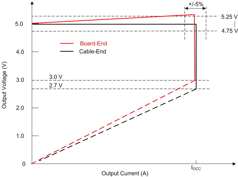 Figure 21. Typical Target Output V-I Curves
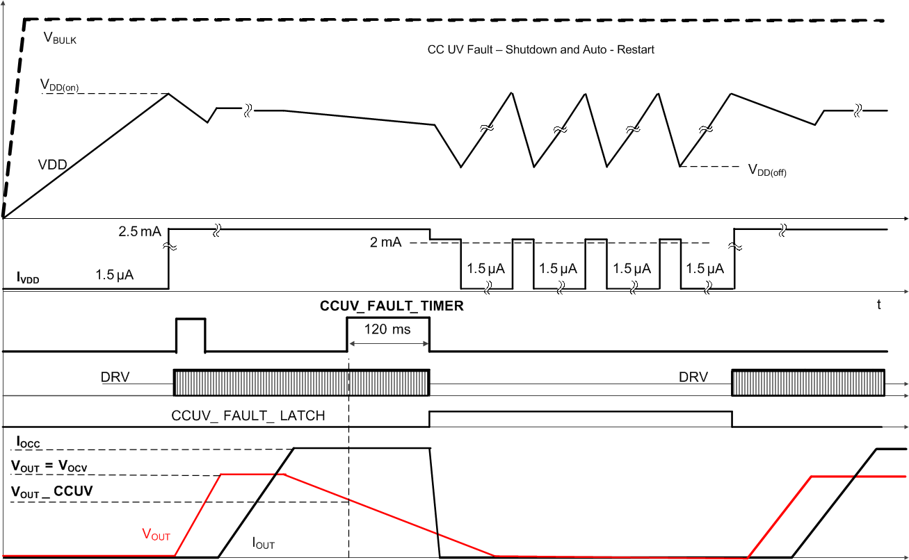 Figure 22. Timing Diagram of CCUV and Output Re-Start
7.3.9 Load Transient Response
The UCC28704 can provide excellent transient performance for most load steps. However the response of PSR controller is always limited by the operating frequency of the converter, since the controller only samples or reads the output voltage once every switching cycle. At zero external load, or standby, the operating frequency is set by any preload together with the bias power needed. This frequency, fSW(standby), sets a maximum incremental response delay. The preload can always be adjusted, at the expense of standby power, to increase the standby frequency. The actual response delay depends on the relative timing of the load step within the switching cycle. Thus for a given load step, IOUT(step), the output deviation can be as large as:

In the case of repeating load transients the situation is aggravated. Whenever the load steps from a modest current level to zero, there is a period of time when there is a slight over-shoot in the output voltage and the control loop saturates and force the converter operating at to its minimum switching frequency, fSW(min), or 1 kHz regardless what preload setting is. If the next positive load step occurs during this time the output deviation will be larger, remembering that fSW(standby) must be > fSW(min).
A special transient response algorithm in this controller dynamically adjusts the minimum controlled switching frequency, such that during a mid to high current level condition the loop's minimum switching frequency is raised to fSW(lim), typically 4 kHz. This raised minimum switching frequency is maintained following a load step-down change until the output voltage rises momentarily to 10% above its normal regulating level or has stayed above its normal regulating level for 500 ms. During this time the response to a load step-up change benefits from the decreased response delay afforded by the 4-kHz switching frequency. This is illustrated in Figure 23. Application Curves provides test results and further description in regarding to this technique.
NOTE
In applications where standby power is not critical the minimum operating frequency of the loop can be kept higher than 4 kHz. In these cases controller will continuously maintain a 4-kHz minimum frequency.
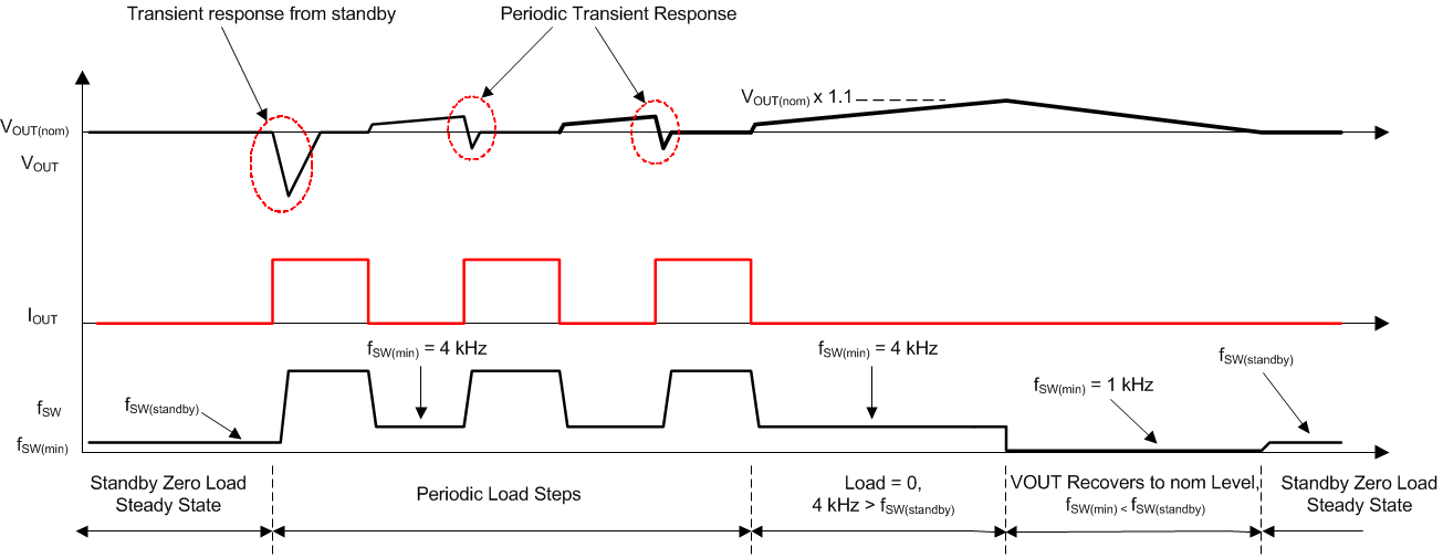 Figure 23. Dynamic Load Response
7.4 Device Functional Modes
The UCC28704 operates in different modes according to input voltage, VDD voltage, and output load conditions:
- At start-up, when VDD is less than the turn-on threshold, VVDD(on) , the device is simply waiting for VDD to reach this threshold while the VDD capacitor is getting charged.
- When VDD exceeds VVDD(on), the device starts switching to deliver power to the converter output. The initial 3 switching cycles control the primary-peak current to IPP(min). This allows sensing any initial input or output faults with minimal power delivery. When confirmed with input voltage above predetermined level and no fault conditions, start up process proceeds and normal power conversion follows. The converter will remain in discontinuous current mode operation during charging of the output capacitor(s), maintaining a constant output current until the output voltage reaches its regulation point.
- CV mode means that the converter keeps the output voltage constant. When the load current is less than the current limit level, the converter operates in CV mode to keep the output voltage at the regulation level over the entire load and input line ranges.
- CC mode means that the converter keeps the output current constant. When the output voltage is below the regulation level, the converter operates in CC mode to limit the output current.
- In CC mode, when the output voltage starts to drop below regulation and if it reaches below the CCUV threshold VCCUV, sensed at the VS pin, the controller declares a CCUV fault and disables PWM. The controller initiates a shutdown-restart operation. This protection mode helps avoid USB terminals from getting over-heated and thereby preventing a burn-out condition, which is also called soft-short protection. Detailed description is in Constant Current Under-Voltage Protection.
- When operating in CV mode where IPP reaches IPP(max), the UCC28704 operates continuously in the run state. In this state, the VDD bias current is always at IRUN plus the average gate-drive current.
- When operating in CV mode where IPP is less than IPP(max), the UCC28704 operates in the wait state between switching cycles and in the run state during a switching cycle. In the wait state, the VDD bias current is reduced to IWAIT after demagnetizing time of each switching cycle to improve efficiency at light loads. This helps reduce light-load power losses, particularly for achieving higher efficiency at 10% and 25% load conditions.
- When a dynamic load change occurs in CV mode, the UCC28704 provides an enhanced transient response to reduce load step caused VOUT dip in periodic load change operation. Detailed description is in Load Transient Response.
- The device operation can be stopped by the events listed below:
- If VDD drops below the VVDD(off) threshold, the device stops switching, its bias current consumption is lowered to ISTART until VDD rises above the VVDD(on) threshold. The device then resumes switching.
- If a fault condition is detected, the device stops switching and its bias current consumption becomes IFAULT. This current level discharges VDD to VVDD(off) where the bias current changes from IFAULT to ISTART until VDD rises above the VVDD(on) threshold.
- By pulling down NTC/SU pin to below VNTCTH, the device responds similar to that of an NTC fault wherein PWM is disabled and converter is shutdown. On releasing the pull-down on NTC, normal operation into CV mode will be restored.
- If a fault condition persists, the operation sequence described above in repeats until the fault condition or the input voltage is removed. Refer to Fault Protection for fault conditions and post-fault operation.