SLUSDD4B April 2019 – December 2020 UC1843B-SP
PRODUCTION DATA
- 1 Features
- 2 Applications
- 3 Description
- 4 Revision History
- 5 Pin Configuration and Functions
- 6 Specifications
- 7 Detailed Description
- 8 Application Information Disclaimer
- 9 Power Supply Recommendations
- 10Layout
- 11Device and Documentation Support
- 12Mechanical, Packaging, and Orderable Information
8.2.3 Application Curves
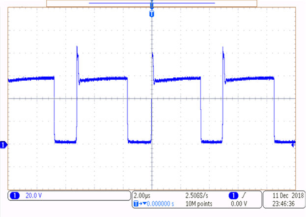
 Figure 8-2 Switch Node of Flyback Converter
For the test in Figure 8-2, 40 V was applied to the input and 10 A was drawn from the output. Ringing can be present on the switching node if the converter is run in discontinuous conduction mode rather than the continuous conduction mode the design was run with.
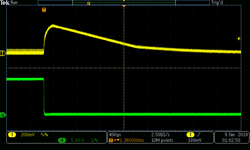
 Figure 8-3 Load Step Down With 40 VIN
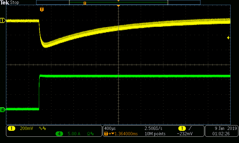
 Figure 8-4 Load Step Up With 40 VIN
For tests shown in and , 40 V was applied to the input and a load step was applied to the output. The load step applied was from 0 A to 10 A and 10 A to 0 A. Note that those currents do not include the 0.1-A pre-load. The curves show that the stability of the design due to the lack of ringing during the load step.