SLUU408A February   2010  – January 2022 TPS51125A


  1.   Trademarks
  2. 1Introduction
  3. 2Performance Specification Summary
  4. 3Schematic
  5. 4Test Setup and Results
    1. 4.1 Test Setup
    2. 4.2 Test Procedure
    3. 4.3 Start-Up Performance
  6. 5Configuration
    1. 5.1 Switching Frequency Selection
    2. 5.2 Operation Mode Selection
    3. 5.3 VCLK ON/OFF Selection
  7. 6Physical Layouts
  8. 7List of Materials
  9. 8References
  10. 9Revision History

Physical Layouts

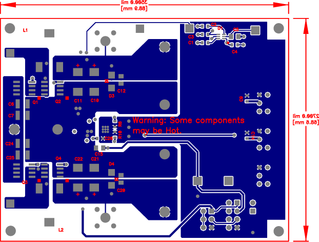
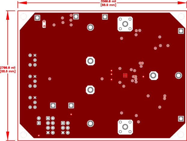
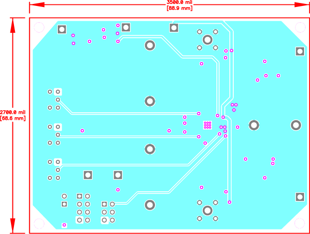
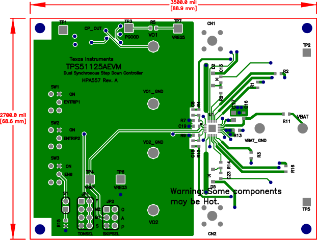
This section provides the board layout and assembly drawings for the EVM, that include the top layer (Figure 6-1), the bottom layer (Figure 6-2), and inner layer views (Figure 6-3 and Figure 6-4) of the EVM.
GUID-FA44F82D-80B6-4A10-AAA3-964ADA7E95DF-low.pngFigure 6-1 Top Layer Routing
GUID-66EB7439-A1D2-47BD-BD7D-B01625DDF723-low.pngFigure 6-2 Bottom Layer Routing
GUID-D58CC3C8-AB4A-4A28-A868-AECB8AD371BD-low.pngFigure 6-3 Inner Layer 1
GUID-B260822F-D6E9-4E45-8BA0-83F6227AAB22-low.pngFigure 6-4 Inner Layer 2