SLUUC04A February   2019  – June 2021 TPS568230


  1.   Trademarks
  2. 1Introduction
  3. 2Performance Specification Summary
  4. 3Schematic and List of Materials
  5. 4Board Layout
  6. 5Bench Test Setup conditions
    1. 5.1 Headers Description and Jumper Placement.
    2. 5.2 Power-Up Procedure
  7. 6Test Waveform
    1. 6.1 Power Up
    2. 6.2 Power Down
    3. 6.3 Output Voltage Ripple
    4. 6.4 Load Transient
    5. 6.5 Thermal
  8. 7Revision History

Power Down

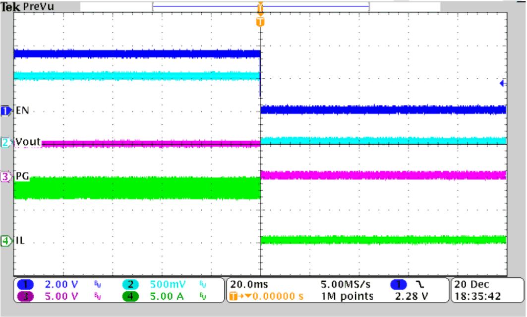
Figure 6-3 and Figure 6-4 show the power down waveforms for the TPS568230EVM board. The applied input voltage is 12 V. Once the EN is down, Vout ramps down.
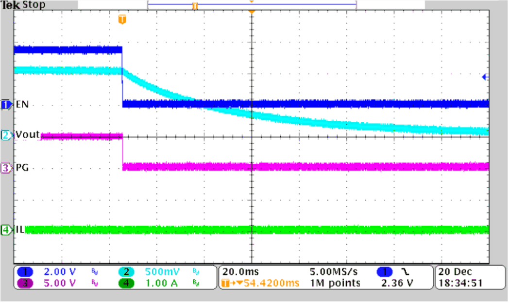
GUID-802C3519-B7C8-4606-B6C6-7889F6F9D1FB-low.gifFigure 6-3 Power Down with 0 A
GUID-31745A7C-A4A6-41D6-9F16-B8BD878273C6-low.gifFigure 6-4 Power Down with 8 A