SLUUC66B May 2020 – April 2021 TPSM5D1806
4 Schematic
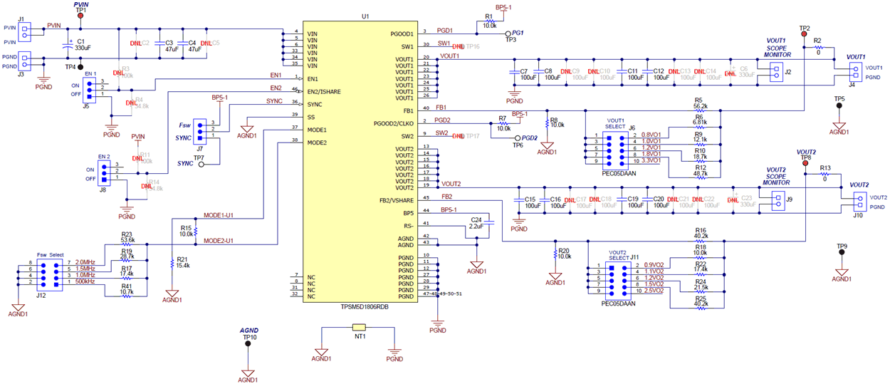
Figure 4-1 is the schematic for the top-half of TPSM5D1806EVM.
 Figure 4-1 TPSM5D1806EVM Independent Dual Output Schematic
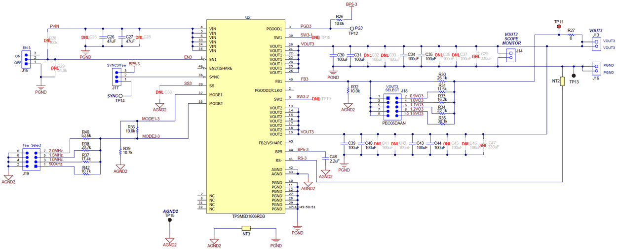
Figure 4-2 is the schematic for the bottom-half of TPSM5D1806EVM.
 Figure 4-2 TPSM5D1806EVM Independent Parallel Output Schematic