SLUUCF8 March 2021
8 Evaluation Module (EVM) Hardware
Board Layout
Figure 8-1 through Figure 8-16 show the TPS53676EVM-084 assembly drawings and TPS53676EVM-084 PCB layout images.
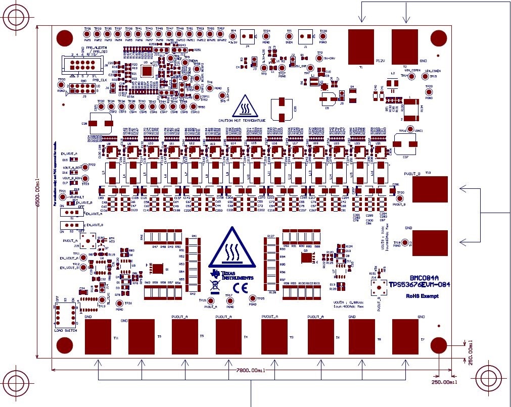 Figure 8-1 TPS53676EVM-084 Assembly
Drawing Top View
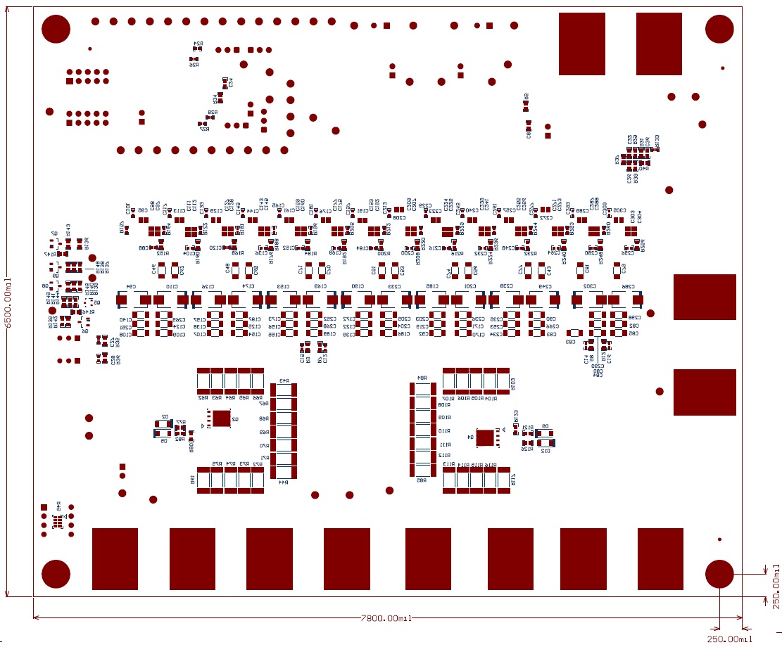 Figure 8-2 TPS53676EVM-084 Assembly
Drawing Bottom View
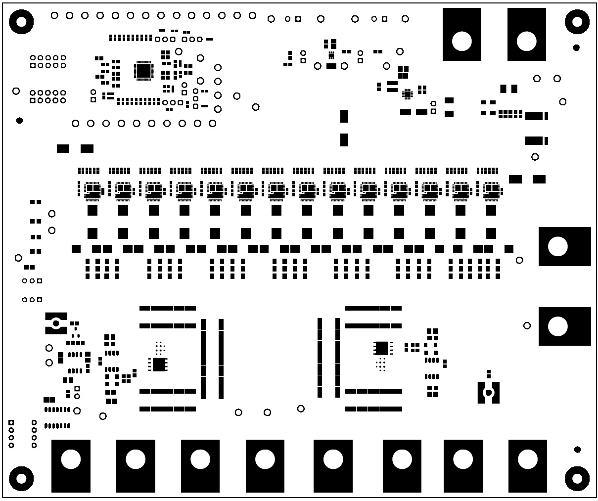 Figure 8-3 TPS53676EVM-084 PCB Top
Solder
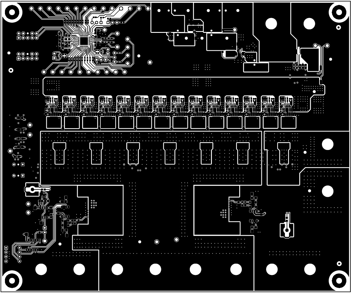 Figure 8-4 TPS53676EVM-084 PCB Top
layer
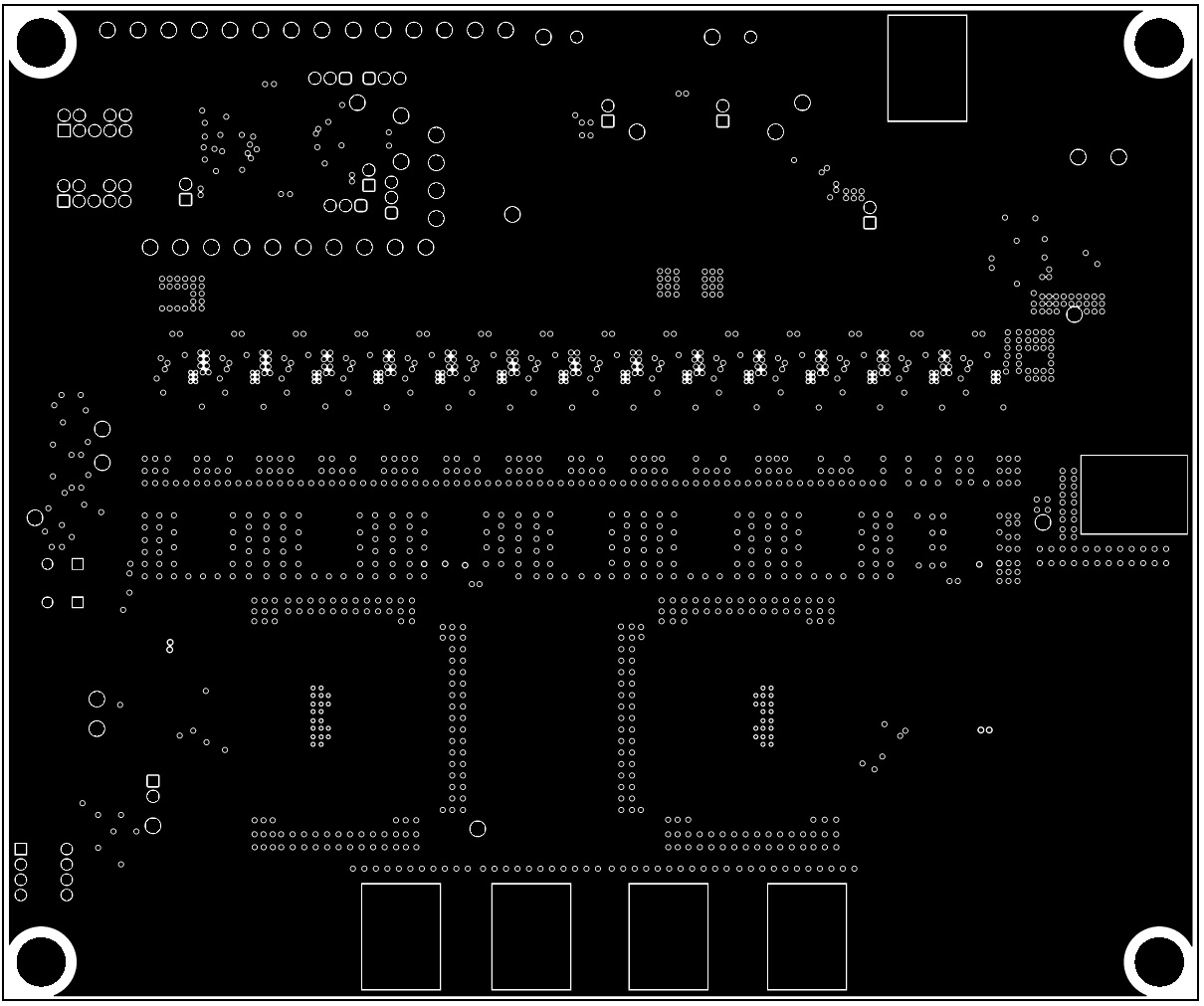 Figure 8-5 TPS53676EVM-084 PCB
Layer2-GND
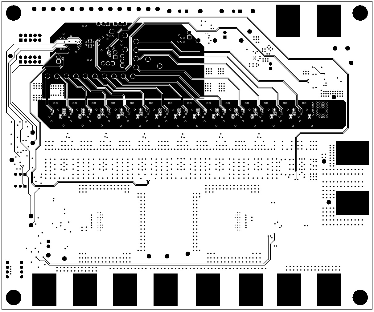 Figure 8-6 TPS53676EVM-084 PCB
Layer03-Signal
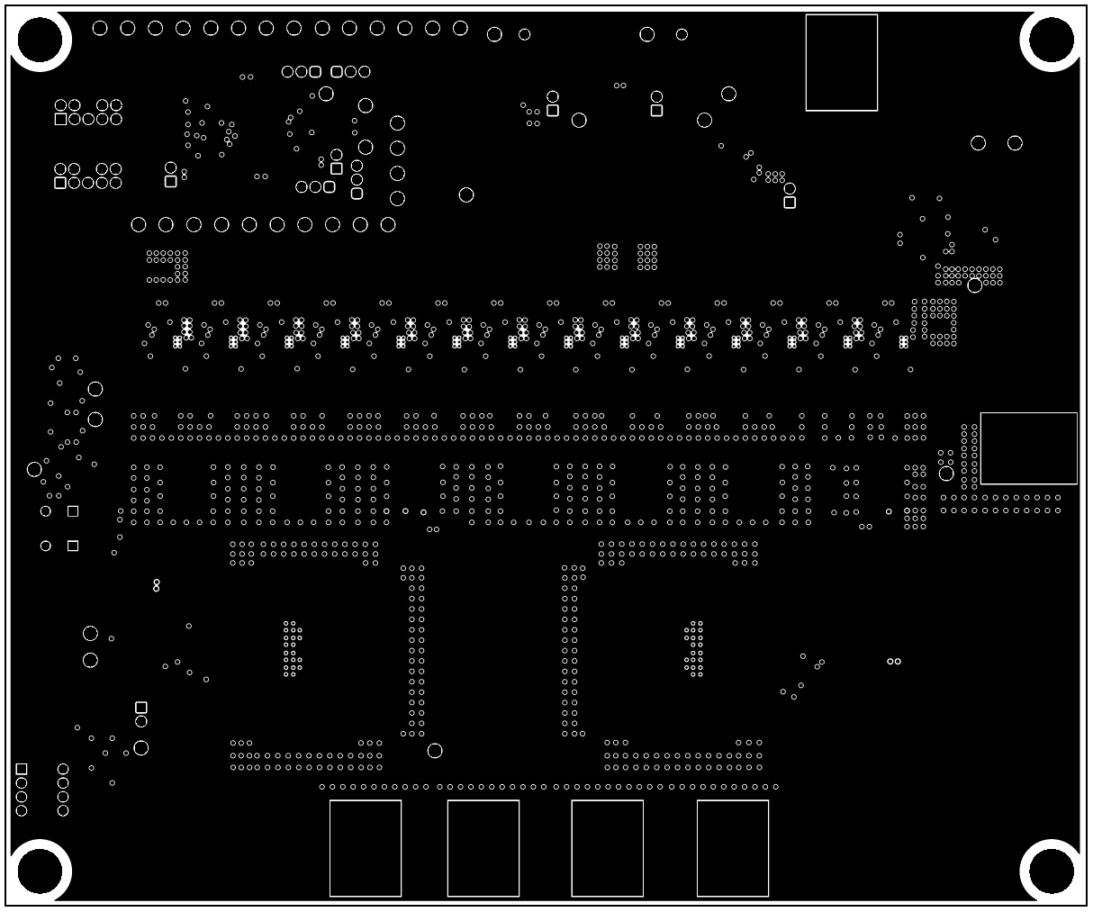 Figure 8-7 TPS53676EVM-084 PCB
Layer04-GND
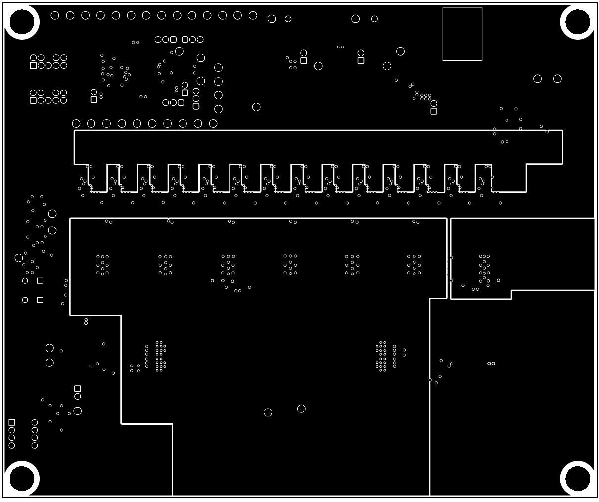 Figure 8-8 TPS53676EVM-084 PCB
Layer05-Power
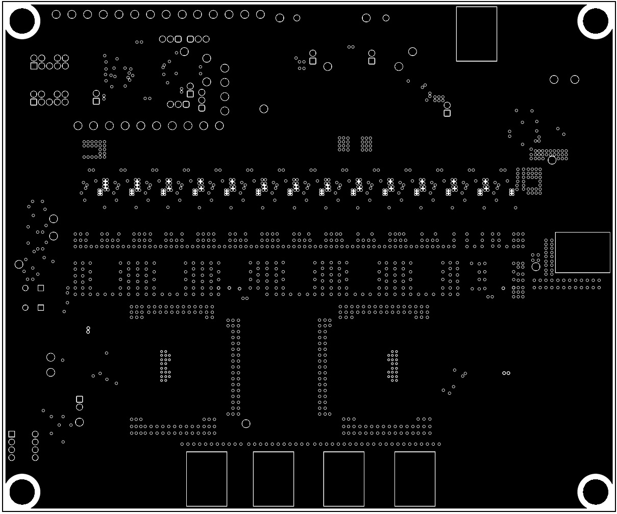 Figure 8-9 TPS53676EVM-084 PCB
Layer06-GND
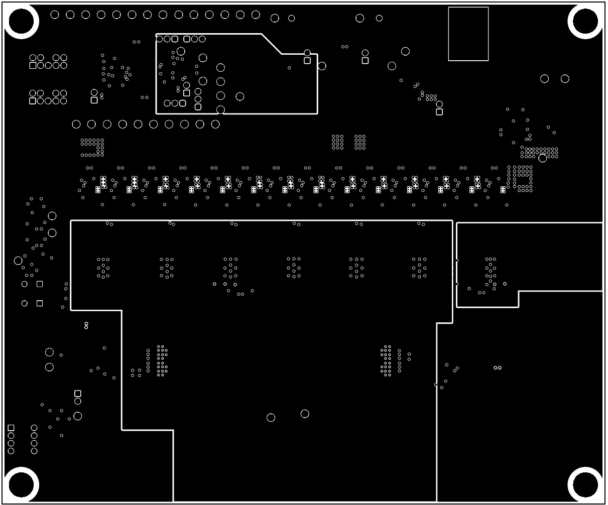 Figure 8-10 TPS53676EVM-084 PCB
Layer07-Power
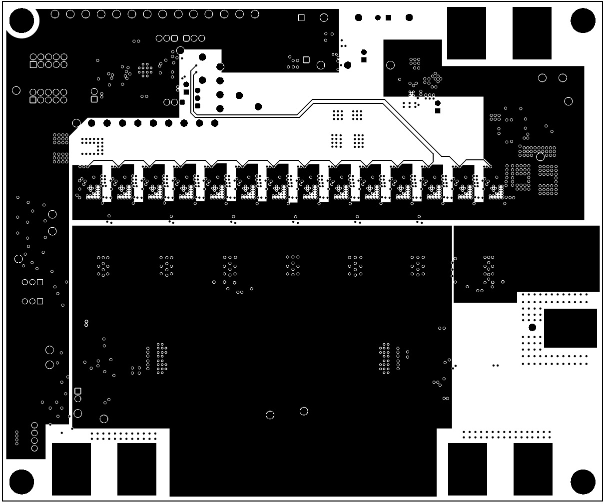 Figure 8-11 TPS53676EVM-084 PCB
Layer08-Power
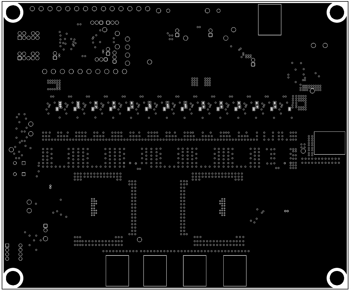 Figure 8-12 TPS53676EVM-084 PCB
Layer09-GND
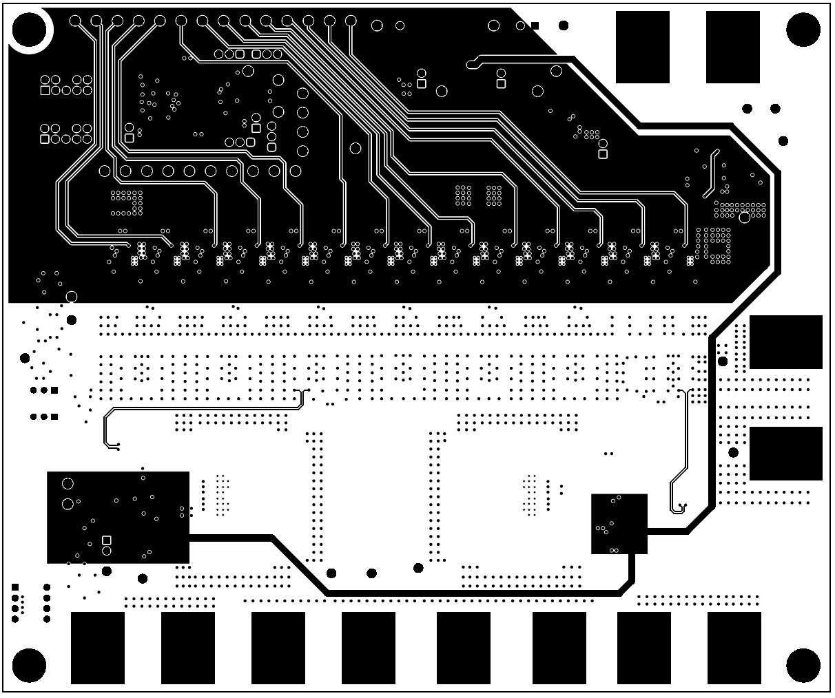 Figure 8-13 TPS53676EVM-084 PCB
Layer10-Signal
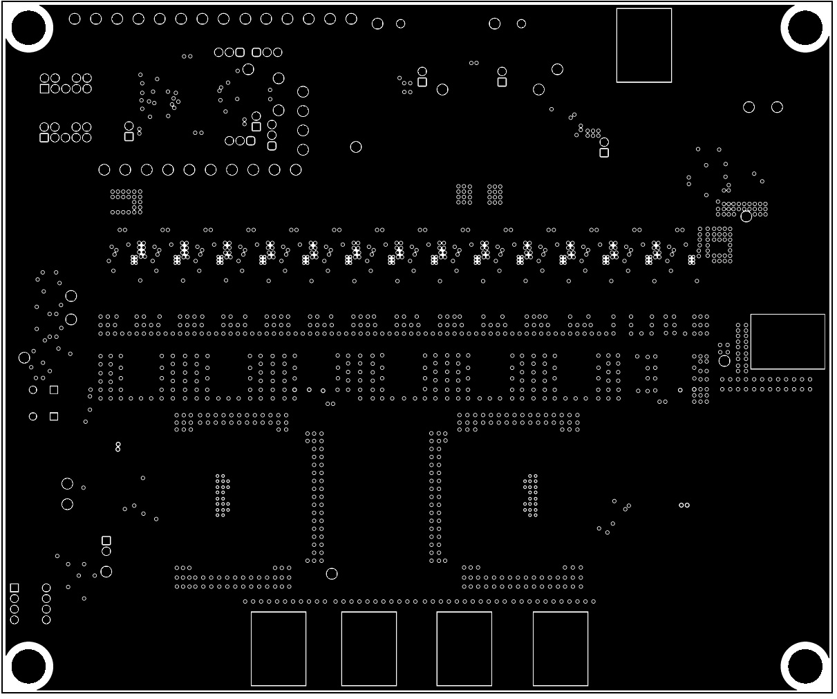 Figure 8-14 TPS53676EVM-084 PCB
Layer11-GND
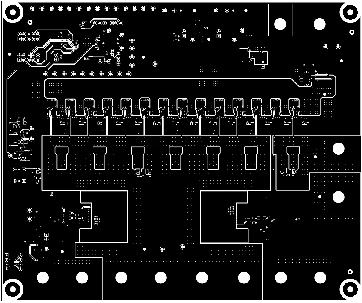 Figure 8-15 TPS53676EVM-084 PCB Bottom
layer
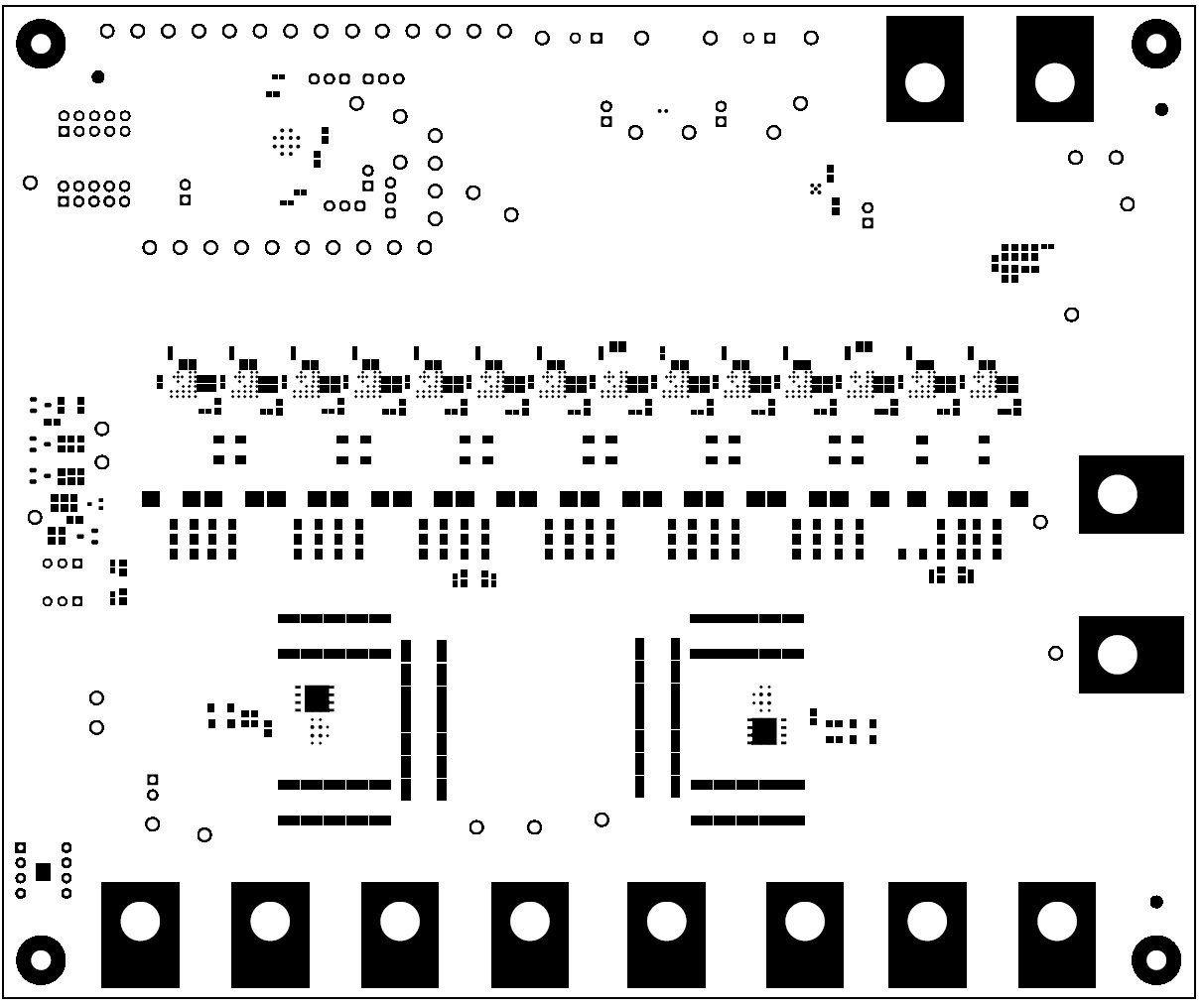 Figure 8-16 TPS53676EVM-084 PCB Bottom
solder