SLUUCG4 November 2022 TPS548C26
2 Performance Characteristics
Table 2-1 provides a summary of the TPS548C26EVM performance characteristics. The TPS548C26EVM is designed and tested for VIN = 8 V to 16 V. Characteristics are given for an input voltage of VIN = 12 V and output voltage of 3.3 V, unless otherwise specified. The ambient temperature is room temperature (20°C to 25°C) for all measurements, unless otherwise noted.
Table 2-1 TPS548C26EVM Performance Characteristics Summary
| SPECIFICATION | TEST CONDITIONS | MIN | TYP | MAX | UNIT | |
|---|---|---|---|---|---|---|
| VIN voltage range | 8 | 12 | 16 | V | ||
| PVIN input current | PVIN = 12 V, internal VCC/VDRV, IO = 0 A, Pulse-skip mode | 15 | mA | |||
| VCC/VDRV input current | External 5-V bias, fSW = 800 kHz, PVIN = 12 V, IO = 35 A | 38 | mA | |||
| Output voltage setpoint | 3.3 | V | ||||
| Output current range | VIN = 8 V to 16 V | 0 | 35 | A | ||
| Output ripple voltage | fSW = 800 kHz, IO = 35 A | 28 | mVPP | |||
| Output rise time | 1 | ms | ||||
| Current limit | Set by J10 | 35 | A | |||
| Switching frequency (fSW) | Set by J11 | 600 | 800 | 1200 | kHz | |
| Efficiency | VIN = 12 V, external 5-V bias, fSW = 800 kHz, IO = 35 A | 91 | % | |||
| IC case temperature | VIN = 12 V, external 5-V bias, fSW = 1.2 MHz, IO = 35 A, 15-minute dwell time | 103 | °C | |||
Figure 2-1 Efficiency, FCCM, Internal
LDO
Figure 2-3 Efficiency, FCCM, External
5-V Bias
Figure 2-5 Efficiency, DCM. Internal
LDO
Figure 2-7 Efficiency, DCM, External
5-V Bias
Figure 2-9 Load Regulation, FCCM,
Internal LDO
Figure 2-11 Load Regulation, DCM,
Internal VCC LDO
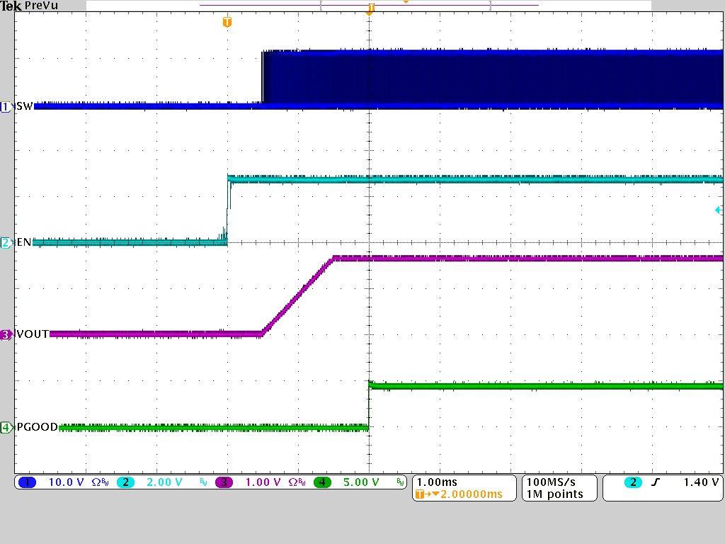 Figure 2-13 ENABLE Start-Up
Waveform
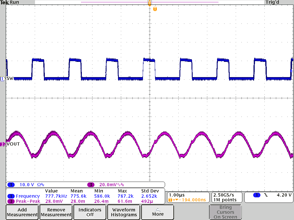 Figure 2-15 Output Voltage Ripple,
800-kHz FCCM, 35-A Load
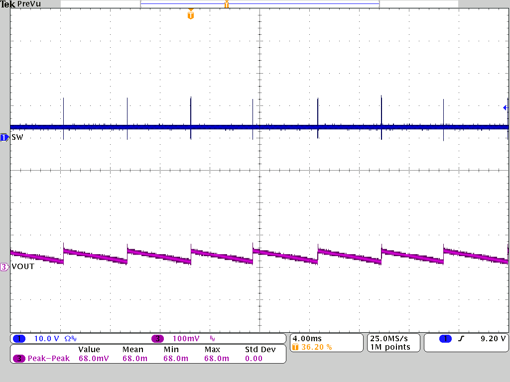 Figure 2-17 Output Voltage Ripple,
DCM, No Load
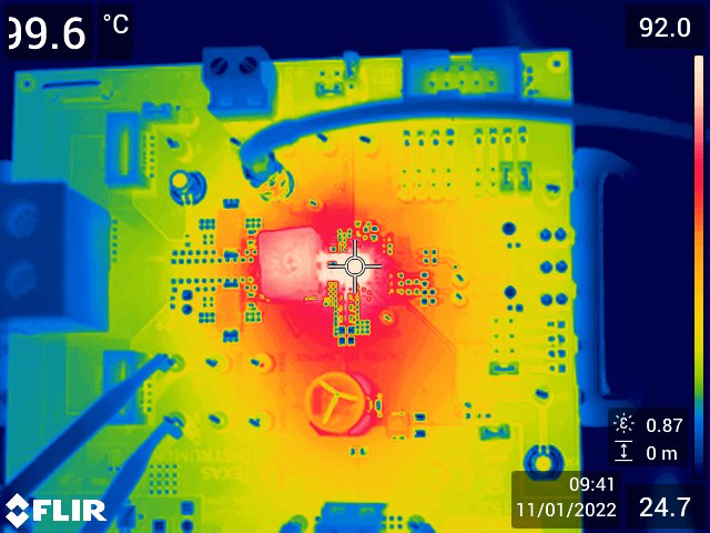 Figure 2-19 Thermal Characteristics,
600-kHz FCCM, Internal LDO, 35-A Load
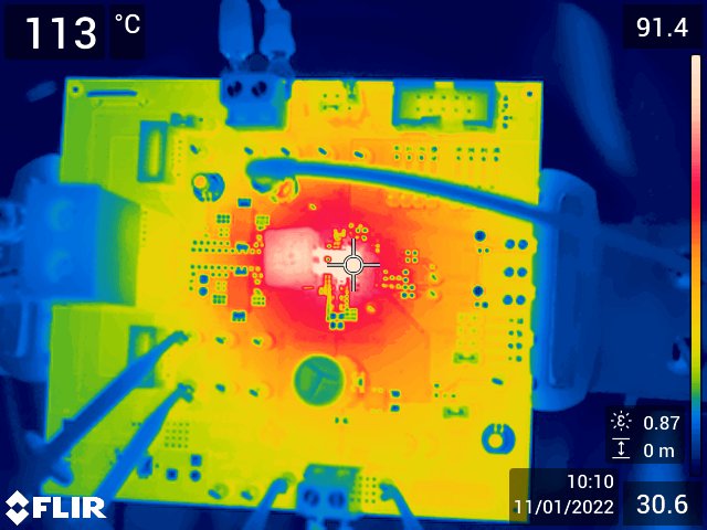 Figure 2-21 Thermal Characteristics,
800-kHz FCCM, Internal LDO, 35-A Load
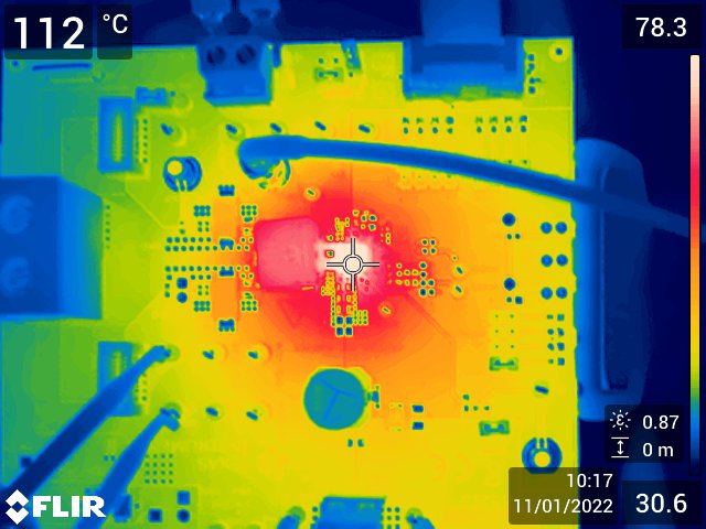 Figure 2-23 Thermal Characteristics,
1.2-MHz FCCM, Internal LDO, 35-A Load
Figure 2-23 Thermal Characteristics,
1.2-MHz FCCM, Internal LDO, 35-A LoadFigure 2-2 Power Dissipation, FCCM,
Internal LDO
Figure 2-4 Power Dissipation, FCCM,
External 5-V Bias
Figure 2-6 Power Dissipation, DCM,
Internal LDO
Figure 2-8 Power Dissipation, DCM,
External 5-V Bias
Figure 2-10 Load Regulation, FCCM,
External 5-V Bias
Figure 2-12 Load Regulation, DCM,
External 5-V Bias
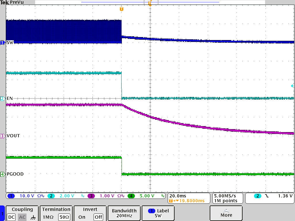 Figure 2-14 ENABLE Shutdown
Waveform
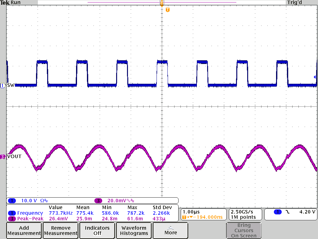 Figure 2-16 Output Voltage Ripple,
800-kHz FCCM, No Load
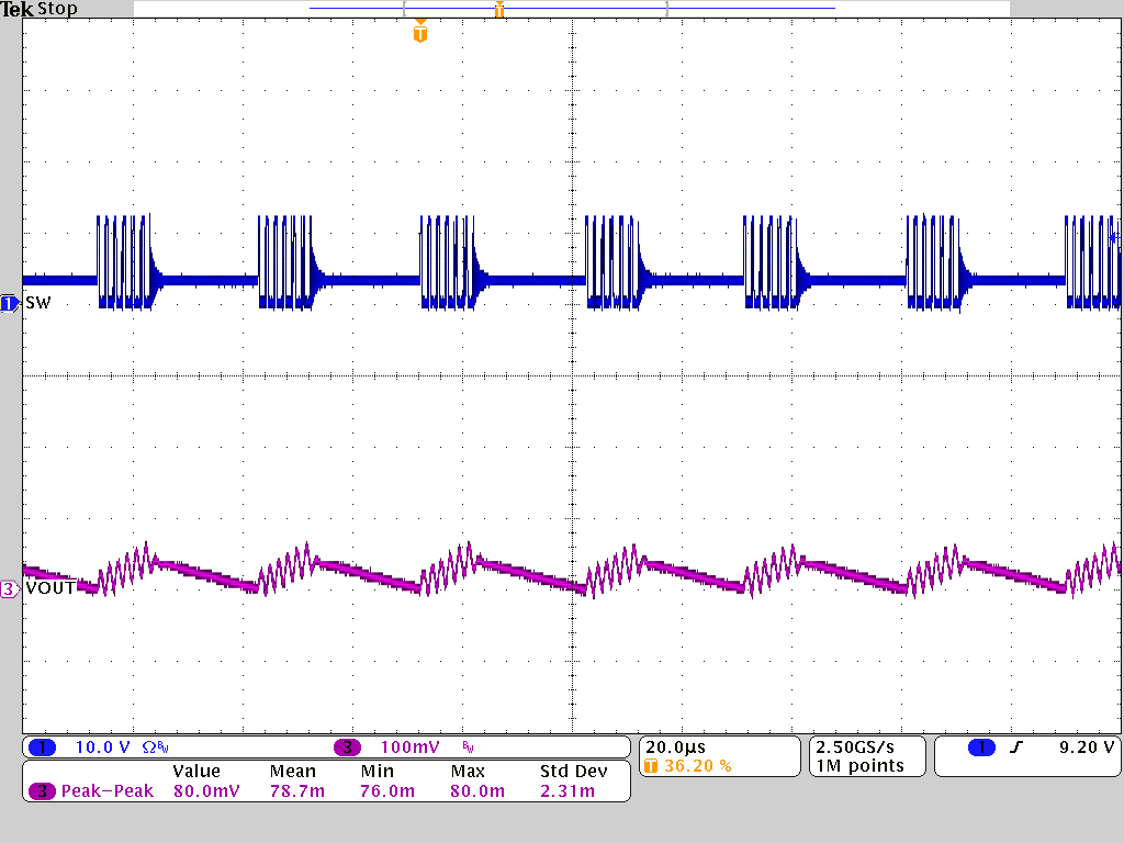 Figure 2-18 Output Voltage Ripple,
DCM, 1-A Load
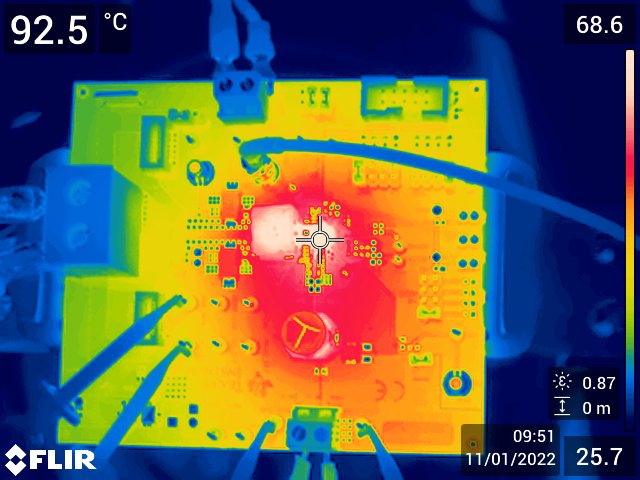 Figure 2-20 Thermal Characteristics,
600-kHz FCCM, External 5-V Bias, 35-A Load
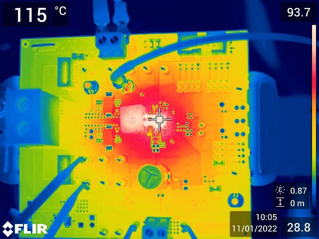 Figure 2-22 Thermal Characteristics,
800-kHz FCCM, External 5-V Bias, 35-A Load
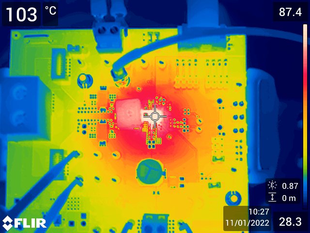 Figure 2-24 Thermal Characteristics,
1.2-MHz FCCM, External 5-V Bias, 35-A Load