SLVA998A November 2018 – July 2021 TPS61322
3.2 Signal Switch Q1
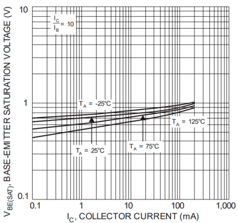
The switch Q1 is a general purpose NPN bipolar transistor to save cost. The Vbe is sensitive to the temperature changes. TI recommends placing the Q1 a little away from the TPS613222A and Q2, which generates some heat during short-circuit protection. This switch can be replaced by a small signal NMOS FET.
The Q1 switch can be a NMOS FET as well. If the Q1 is NMOS, then the leakage current is negligible because of the high impedance from the gate to source. And the response time will be very short but the recovery time will be very long because of the small leakage current.
 Figure 3-1 MMBT3904 I-V Curve See References no. 2