SLVAET6A June 2020 – June 2020 TPS7H4001-SP
2 BOM Modifications Required
The following steps must be taken to ensure proper operation of a 2-channel buck converter on a populated 4-channel EVM (TPS7H4001QEVM-CVAL). An overview of where changes are required is shown in Figure 2 while a summary of all changes is provided in Table 1.
Figure 2. Overview Of Required Modifications 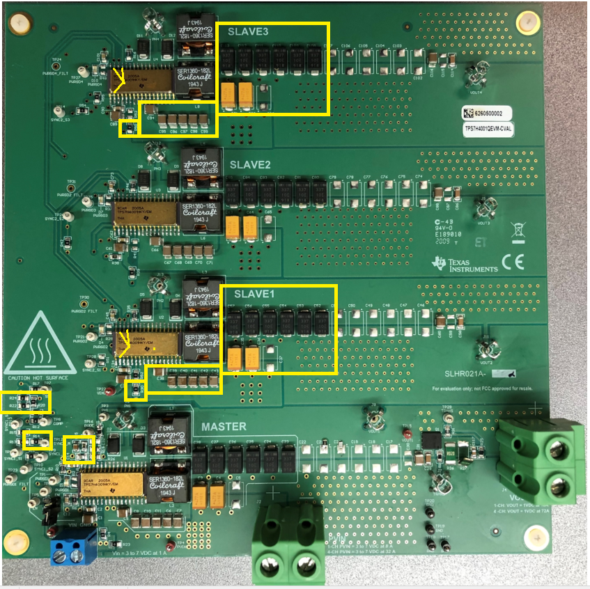

- Modifications near MASTER DUT U1 (Figure 3 and Figure 8)
- Isolate VSENSE feedback pins 32 of SLAVE1 and SLAVE3 by removing 0-ohm jumpers R20 and R24, respectively.
- Isolate SYNC2 pin 6 of slave devices by removing 0-ohm jumper R14
- Replace soft start capacitor, C13, with 22nF to keep soft start at 2ms.
- Replace compensation circuit at R7, C14, C15 near DUT U1:
- R7=6.04kohms
- C15=18nF
- C14=180pF
- Modifications near SLAVE1 DUT U2 (Figure 4 and Figure 9)
- Isolate VIN pin 4 of Slave 1 DUT U2 by removing 0-ohm jumper R30
- Remove input capacitors of Slave 1 DUT U2 by completely removing, or lifting one terminal of each capacitor as shown in Figure 5. (C35, C36, C38, C39, C40, C41, C42, C43)
- Remove output capacitors of Slave 1 DUT U2 by completely removing, or lifting one terminal of each capacitor so as to remove from circuit as shown in Figure 5. (C52, C53, C54, C55, C56, C57, C58, C60)
- Using a solder iron and tweezers, carefully lift the following pins off the PCB as shown in Figure 6 (note only pins 31 and 33 are shown in graphic)
- Enable pin (EN pin2)
- Soft start pin (SS/TR pin31)
- COMP pin (COMP pin 33)
- Modifications near SLAVE3 DUT U4 (Figure 7 and Figure 11)
- Isolate VIN pin 4 of Slave 3 DUT U4 by removing 0-ohm jumper R50
- Remove input capacitors of Slave 3 DUT 4 by completely removing, or lifting one terminal of each capacitor as shown in Figure 5. (C91, C92, C94, C95, C96, C97, C98, C99)
- Remove output capacitors of Slave 3 DUT U4 by completely removing, or lifting one terminal of each capacitor so as to remove from circuit as shown in Figure 5. (C108, C109, C110, C111, C112, C113, C114, C116)
- Using a solder iron and tweezers, carefully lift the following pins off the PCB as shown in Figure 6 (note only pins 31 and 33 are shown in graphic)
- Enable pin (EN pin2)
- Soft start pin (SS/TR pin31)
- COMP pin (COMP pin 33)
Figure 3. Modifications Near MASTER DUT U1 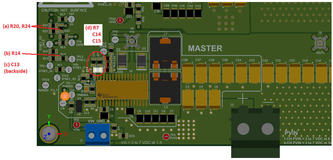

Figure 4. Modifications near SLAVE1 DUT U2

Figure 5. Open Circuit Input/Output Capacitors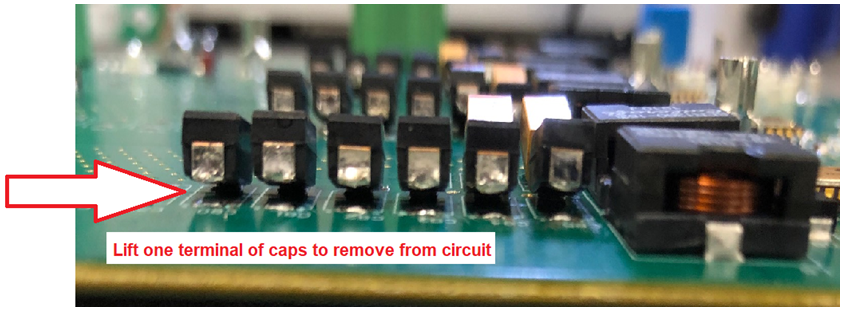

Figure 6. Lift Pins 2, 31, 33 from PCB 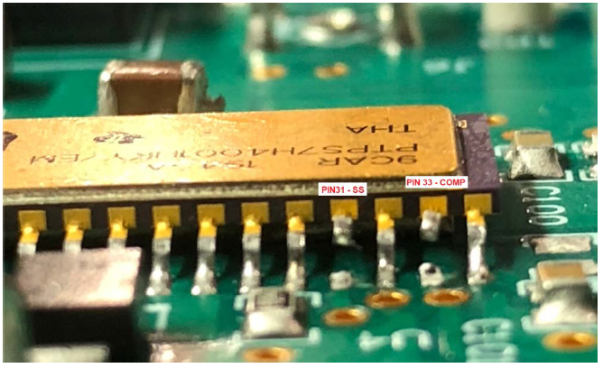

Figure 7. Modifications near SLAVE3 DUT U4 

Table 1. Summary of BOM Changes
| Position on PCB | Component Designator | Action |
|---|---|---|
| MASTER DUT U1 | R14, R20, R24 | DNI |
| R7 | Replace with 6.04kohms | |
| C14 | Replace with 180pF | |
| C15 | Replace with 18nF | |
| C13 | Replace with 22nF | |
| SLAVE1 DUT U2 | R30 | DNI |
| C35, C36, C38, C39, C40, C41, C42, C43 | DNI | |
| C52, C53, C54, C55, C56, C57, C58, C60 | DNI | |
| U2 pin 2 (EN) | Lift off of PCB | |
| U2 pin 31 (SS/TR) | Lift off of PCB | |
| U2 pin 33 (COMP) | Lift off of PCB | |
| SLAVE3 DUT U4 | R50 | DNI |
| C91, C92, C94, C95, C96, C97, C98, C99 | DNI | |
| C108, C109, C110, C111, C112, C113, C114, C116 | DNI | |
| U3 pin 2 (EN) | Lift off of PCB | |
| U3 pin 31 (SS/TR) | Lift off of PCB | |
| U3 pin 33 (COMP) | Lift off of PCB |