SLVAF46A May 2021 – January 2023 TPS65988
2.1 Thermal Considerations
Face plate is the only means for dissipating the heat generated inside a gang box. Hence, focus should be given in selecting components with less power dissipation. In integrated wall socket designs, the maximum output power of USB ports are capped by the efficiency of ACDC and DCDC regulators. The power dissipated in TPS665988DH’s internal power switch with Rdson of 28m Ω (at Junction temperature of 84℃) is very less compared to the heat contributed by the aforementioned components on the power path. The junction temperature calculation at ambient temperature of 65℃ shows that TPS665988DH is well below the max junction temperature of 150℃.
- Ambient temperature inside the Gang box (mainly contributed by ACDC transformer) (Ta) = 65℃
- Junction-to-ambient thermal resistance of TPS65988DH (RθJa) = 36.4℃/W
- Power dissipation on internal power paths due to IPPHV(continuous current through power path from PP_HVx to VBUSx) of 3A = Rdson * Iout * Iout = 28 m Ω * 3 A * 3A = 252 mW.
- Total power dissipation from both power paths = 504 mW
- Total power dissipation (considering GPIO leakage and active power IVIN_3V3 ) P ~= 520mW
- Junction temperature = Ta + (RθJa * P) = 65 ℃ + (36.4℃/W * 0.52W) = 83.9℃
The Junction temperature can be brought down to a lower value by careful PCB design as recommended in the data sheet.
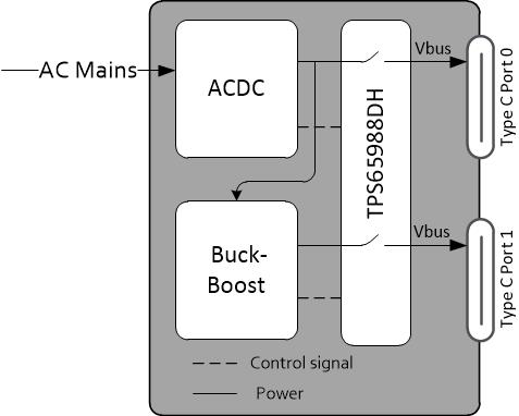
The above thermal calculation is considering the architecture (shown in Figure 2-3), which uses internal power paths of the TI PD controller. In this design, the Buck-Boost regulator is fed from the output of ACDC regulator. Therefore, the ACDC regulator is required to maintain the minimum voltage required for the Buck-Boost regulator to operate. The I2C master of PD controller can be programmed to configure the regulators to supply fixed DC voltage based on the PD negotiation on the respective ports. More details on configuring TPS665988DH’s I2C master to trigger slave write on specific PD events can be found Using I2C Master in TPS65987D and TPS65988 PD Controllers application report.
 Figure 2-3 Dual Port Integrated Type-C PD Wall Socket Architecture Using TPS665988DH’s Internal Power Switch