SLVAF47 March 2021 TPS7H4001-SP
5 ADA-SDEV-KIT2 Platform
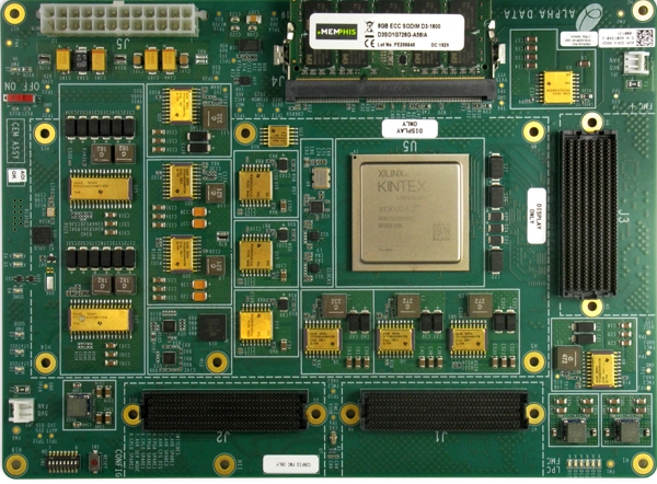
With the ADA-SDEV-KIT2 platform from Alpha Data Parallel Systems, you can evaluate the KU060 (the commercial package) alongside a space-rated power solution from Texas Instruments. The platform also allows you to test the interaction of the KU060 with other devices (such as high-speed analog-to-digital converters) through its FPGA mezzanine card connectors. Figure 5-1 shows a picture of the ADA-SDEV-KIT2.
 Figure 5-1 The ADA-SDEV-KIT2 Platform for
the KU060
Figure 5-1 The ADA-SDEV-KIT2 Platform for
the KU060To test the performance of the TI-based power supply on the ADA-SDEV-KIT2 platform, Texas Instruments and Alpha Data Parallel Systems performed a large amount of testing using a modified version of the ADA-SDEV-KIT2 kit that used the XQRKU060 (ceramic package) instead of the KU060 (commercial package).
The testing focused on two aspects:
- Assessing the behavior of the XQRKU060 ceramic package and correlating it to the expectations of the GND pins resistance discussed in this paper.
- Validating the approach shown in Table 5-1 (nonuse of the GND_SENSE pin) in DC and AC conditions.
To validate the first aspect, the testing focused on measuring the GND_SENSE pin voltage using two different bitstreams to calculate RGND_SENSE. The bitstreams were generated in a way that the FPGA would require a current from the VCCINT rail large enough to generate a voltage at the GND_SENSE pin. Table 5-1 lists the main features for these two bitstreams. All of the measurements were in DC conditions.
| Bitstream No. 1 | Bitstream No. 2 | ||
|---|---|---|---|
| Clock rate | 13%, 150 MHz | 7%, 200 MHz | |
| Logic usage | 81% | 24% | |
| Block random access memory usage | 0 | 47% | |
| Digital signal processor usage | 0 | 19% | |
| Gigabit transceiver usage | 0 | 0% | |
| Peak VCCINT core current | ≅9 A | ≅25 A | |
| XPE VCCINT voltages | Minimum | 0.917 V | 0.922 V |
| Maximum | 0.993 V | 0.998 V | |
For the resistance calculations, the COMP pin voltage in the TPS7H4001-SP approximated the current corresponding to each bitstream shown in Table 5-1, approximately 9 A and 25 A. The COMP pin voltage correlates to the peak output current from the power stage of the device. These current approximations were also very closely aligned with the VCCINT and VCCINT_IO currents obtained from XPE (VCCINT and VCCINT_IO are internally connected in the XQRKU060, as indicated in the data sheet).
The data after this testing resulted in RGND_SENSE values of 0.25 mΩ and 0.36 mΩ for the approximately 9-A and 25-A bitstreams, respectively. This agrees with the expectations that GND signals and planes are typically the least resistive in ceramic packages given the large number of pins and planes used.All tested cases met the DC regulation requirements for the VCCINT in the XQRKU060, as validated by XPE and Vivado software.
Writing bitstream No. 1 into the external configuration flash memory of the ADA-SDEV-KIT2 validated the AC regulation. The FPGA was cleared and then configured from the flash memory in a constant loop. The DONE signal from the FPGA connected to a diode was used as a trigger to capture the AC transients.
The signals captured were VCCINT, GND, VCCINT_SENSE and GND_SENSE. The first two signals were captured across a decoupling capacitor under the FPGA. The SENSE signals were captured using 0-Ω resistor footprints (not populated for the ceramic package version of the KU060) under the FPGA that provided connection to the VCCINT_SENSE and GND_SENSE pins. For reference, Table 5-2 lists the VCCINT decoupling capacitors used in the ADA-SDEV-KIT2. This capacitance does not include the decoupling capacitors used for the TPS7H4001-SP.
| Capacitor value (µF) | Quantity |
|---|---|
| 680 | 3 |
| 100 | 5 |
| 47 | 13 |
| 4.7 | 10 |
| 1 | 16 |
| 0.22 | 55 |
While in the unprogrammed state, the VCCINT rail in the ADA-SDEV-KIT2 FPGA consumes approximately 0.5 A. This means that each time the FPGA was either configured or cleared, approximately a 8.5-A transient would occur.
Figure 5-2 shows scope shots of the VCCINT response with respect to GND, while Figure 5-3 shows scope shots of the VCCINT_SENSE response with respect to GND_SENSE. In both cases, the load-step responses meet the ±38-mV regulation requirement from XPE as shown in Table 5-1 (0.917 V-0.993 V).