SLVAFC5 March 2022 TPS629210 , TPS629210-Q1
4 Layout Considerations
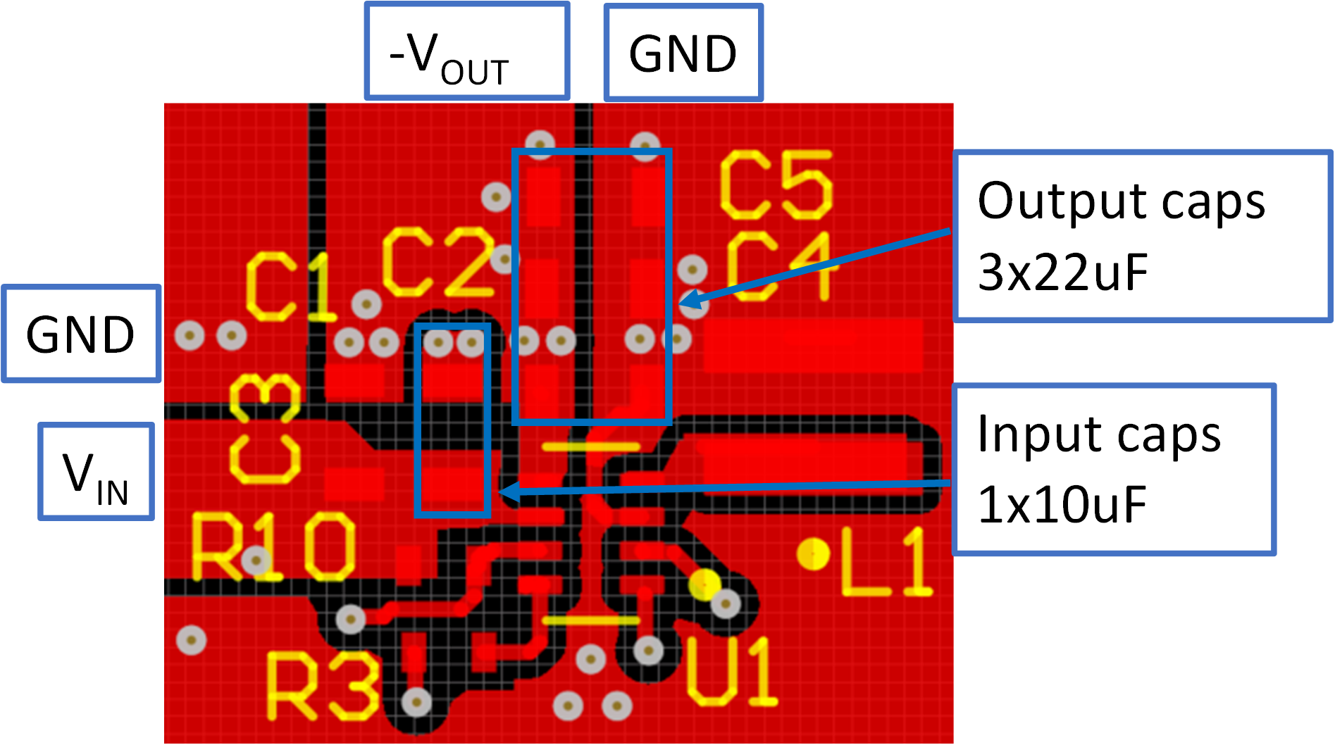
A proper layout is critical for the operation of inverting buck - boost topology. See Figure 4-1 for recommended layout for TPS629210-Q1 inverting buck - boost application.
- The input capacitor C1 should be placed as close as possible between the VIN pin and GND.
- The output capacitors C2, C4, C5 should be placed as close as possible between -VOUT pin and GND.
- VOS trace should be routed/Kelvined to the positive terminal (GND) of output capacitors, not simply tied to the system GND plane.
- Sensitive nodes like FB/VSET and VOS need to be connected with short wires and not nearby high dv/dt signals( like SW). As they carry information about output voltage, they should be connected as close as possible to actual output voltage (at the pad of output capacitor). For this design, there is no feedback resistors required (float the FB/VSET pin) resulting in a -3.3V output voltage using the internal VSET.
- MODE/S-CONF pin resistor R3 should be kept close to IC and connect directly to its pin.
 Figure 4-1 TPS629210-Q1 Inverting Buck –
Boost Layout Example