SLVAFL3 april 2023 BQ25890H
- Abstract
- Trademarks
- 1Introduction
-
2DPDM Structure of BQ25890H
- 2.1 DPDM Block Diagram and Working Flow Chart
- 2.2 Key Register Configuration for BC1.2/HVDCP Standard Power Source with DPDT Signal Switch
- 2.3 Key Register Configuration for BC1.2/HVDCP Standard Power Source Without DPDT Signal Switch
- 2.4 Fast Charging Configuration for PPS/HVDCP Power Source with BQ25890H
- 3References
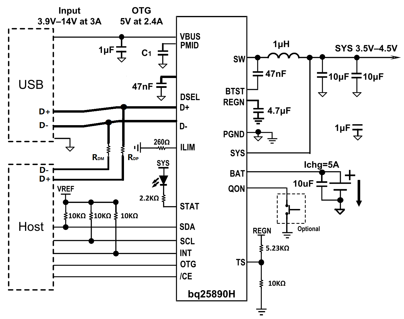
2.3 Key Register Configuration for BC1.2/HVDCP Standard Power Source Without DPDT Signal Switch
 Figure 2-4 Typical Simple Schematic
Without DPDT Switch
Figure 2-4 Typical Simple Schematic
Without DPDT SwitchSometimes, for lower cost consideration, DPDT switch is saved, so the DPDM pin of BQ25890H will be connected to AP(Host) and USB port by RDP and RDM resistor, please note, the resistance of RDP and RDM must be adjusted according to eye-diagram quality of USB signal.
Step1:
When AC adapter is plugged in PD, BQ25890H can start AC adapter identification process, keep
REG02, Bit 0=1, enable Auto DPDM detection (keep default)
Description:
Bit0: Automatic D+/D- Detection Enable
0 –Disable D+/D- or PSEL detection when VBUS is plugged-in
1 –Enable D+/D- or PEL detection when VBUS is plugged-in (default)
Step2:
After identification, BQ25890H will send out INT to AP, then AP will get type of adapter by reading,
REG0B Bit5 to Bit7
Bit description:
VBUS Status register
000: No Input
001: USB Host SDP
010: USB CDP (1.5A)
011: USB DCP (3.25A)
100: Adjustable High Voltage DCP (MaxCharge) (1.5A)
101: Unknown Adapter (500mA)
110: Non-Standard Adapter (1A/2A/2.1A/2.4A)
111: OTG Note: Software current limit is reported in IINLIM register
Step3:
AP (Host) will configure BQ25890H charging profile and start charging process according to type of AC adapter.