SLVK117 October 2022 TPS7H2221-SEP
- Single-Event Effects Test Report of the TPS7H2221-SEP Load Switch
- Trademarks
- 1 Introduction
- 2 Single-Event Effects (SEE)
- 3 Device and Test Board Information
- 4 Irradiation Facility and Setup
- 5 Depth, Range and LETEFF Calculation
- 6 Test Setup and Procedures
- 7 Destructive Single-Event Effects (DSEE)
- 8 Single-Event Transients (SET) and Single Event Functional Interrupt (SEFI)
- 9 Event Rate Calculations
- 10Summary
- A Appendix: Total Ionizing Dose from SEE Experiments
- B Appendix: References
3 Device and Test Board Information
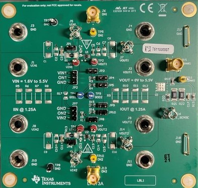
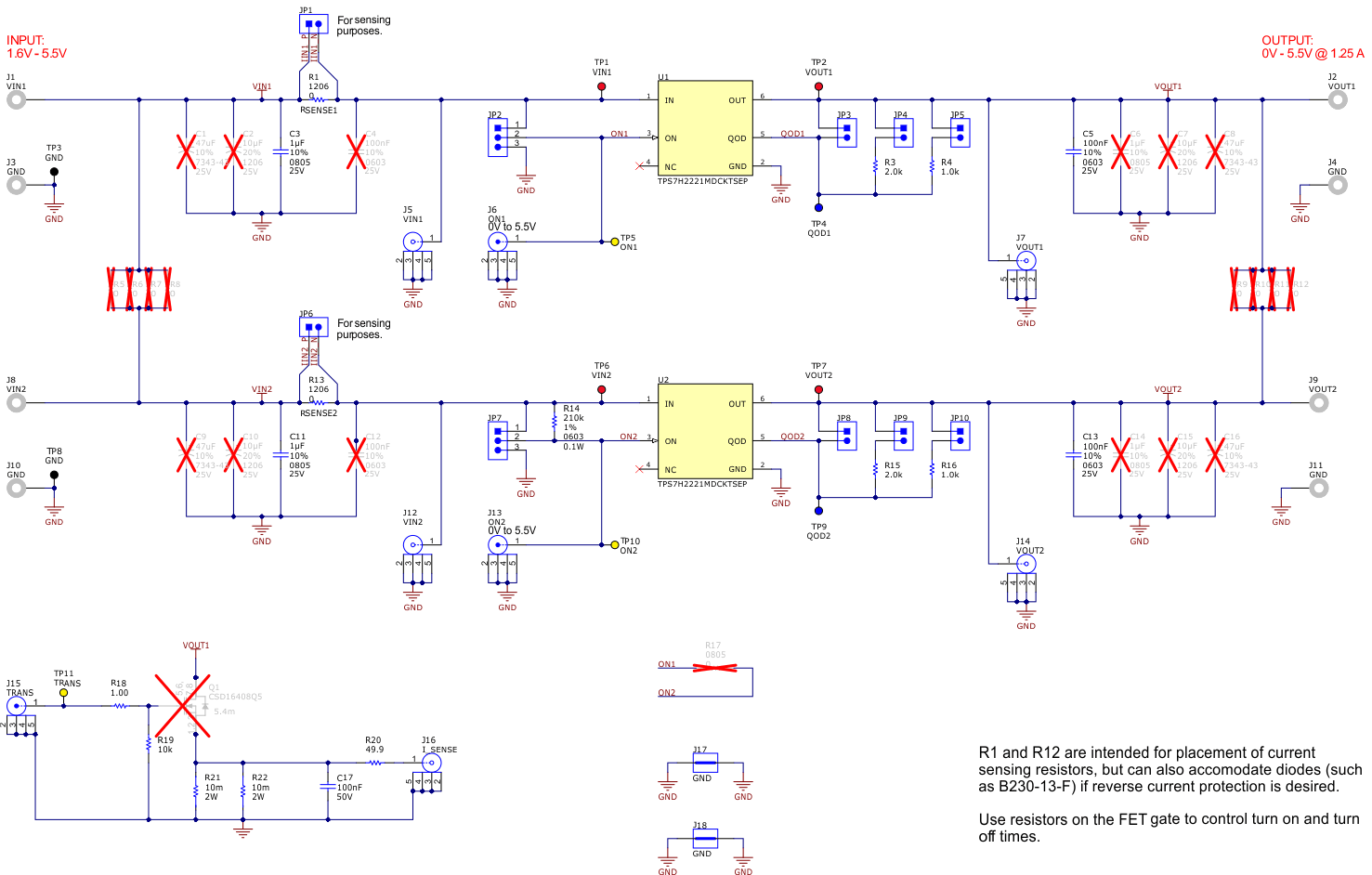
The TPS7H2221-SEP is packaged in a DCK 6-pin SC70 plastic package as shown in Figure 3-1. The TPS7H2221 EVM was used to evaluate the performance and characteristics of the TPS7H2221-SEP under heavy-ions. Figure 3-2 shows the top view of the board used for the radiation testing. Figure 3-4 shows the board schematics used for the heavy-ion testing campaign.
 Figure 3-2 TPS7H2221-SEP Board Top View.
 Because this device is a flip chip a hole was drilled in the board and SEE testing was done "from the back". The ability to see the exposed die through the hole was validated on all EVMs prior to SEE testing. Since the board is dual-site both units were verified and used for testing while under the beam. The boards used for these experiments were modified from the orderable EVM specifically for the test cases discussed in this report and to allow for full dual-site capabilities. For any testing done with the orderable EVM only the bottom circuit (U2) can be used as drilling a hole at U1 would isolate the GND pin from the board.
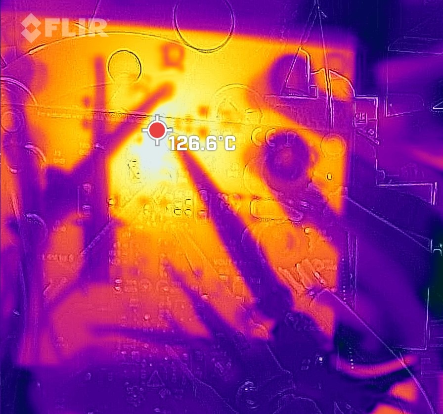
 Figure 3-3 TPS7H2221-SEP Thermal Image for SEL.
  Figure 3-4 TPS7H2221EVM Schematic