SLVS413K October 2002 – July 2022 TPS61040 , TPS61041
PRODUCTION DATA
- 1 Features
- 2 Applications
- 3 Description
- 4 Revision History
- 5 Pin Configuration and Functions
- 6 Specifications
- 7 Detailed Description
- 8 Application and Implementation
- 9 Power Supply Recommendations
- 10Layout
- 11Device and Documentation Support
- 12Mechanical, Packaging, and Orderable Information
3 Description
The TPS6104x is a high-frequency boost converter dedicated for small to medium LCD bias supply and white LED backlight supplies. The device is ideal to generate output voltages up to 28 V from a dual-cell NiMH/NiCd or a single-cell Li-Ion battery. The part can also be used to generate standard 3.3-V or 5-V to 12-V power conversions.
The TPS6104x operates with a switching frequency up to 1 MHz. This frequency allows the use of small external components using ceramic as well as tantalum output capacitors. Together with the thin WSON package, the TPS6104x gives a very small overall solution size. The TPS61040 device has an internal 400-mA switch current limit, while the TPS61041 device has a 250-mA switch current limit, offering lower output voltage ripple and allows the use of a smaller form factor inductor for lower power applications. The low quiescent current (typically 28 μA) together with an optimized control scheme, allows device operation at very high efficiencies over the entire load current range.
| PART NUMBER | PACKAGE(1) | BODY SIZE (NOM) |
|---|---|---|
| TPS61040 | SOT-23 (5) | 2.90 mm × 1.60 mm |
| SOT (5) | 2.90 mm ×1.60 mm | |
| WSON (6) | 2.00 mm × 2.00 mm | |
| TPS61041 | SOT-23 (5) | 2.90 mm ×1.60 mm |
| WSON (6) | 2.00 mm × 2.00 mm |
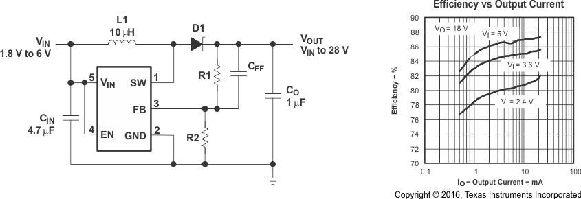
 Typical
Application Schematic