SLVS632K January 2006 – January 2024 TPS5430 , TPS5431
PRODUCTION DATA
- 1
- 1 Features
- 2 Applications
- 3 Description
- 4 Pin Configuration and Functions
- 5 Specifications
-
6 Detailed Description
- 6.1 Overview
- 6.2 Functional Block Diagram
- 6.3
Feature Description
- 6.3.1 Oscillator Frequency
- 6.3.2 Voltage Reference
- 6.3.3 Enable (ENA) and Internal Slow Start
- 6.3.4 Undervoltage Lockout (UVLO)
- 6.3.5 Boost Capacitor (BOOT)
- 6.3.6 Output Feedback (VSENSE) and Internal Compensation
- 6.3.7 Voltage Feed-Forward
- 6.3.8 Pulse-Width-Modulation (PWM) Control
- 6.3.9 Overcurrent Limiting
- 6.3.10 Overvoltage Protection
- 6.3.11 Thermal Shutdown
- 6.4 Device Functional Modes
-
7 Application and Implementation
- 7.1 Application Information
- 7.2
Typical Applications
- 7.2.1
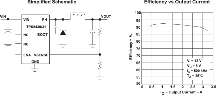
12-V Input to 5.0-V Output
- 7.2.1.1 Design Requirements
- 7.2.1.2 Detailed Design Procedure
- 7.2.1.3 Application Curves
- 7.2.2 Wide Input Voltage Ranges with TPS5430
- 7.2.3 Circuit Using Ceramic Output Filter Capacitors
- 7.2.1
12-V Input to 5.0-V Output
- 7.3 Power Supply Recommendations
- 7.4 Layout
- 8 Device and Documentation Support
- 9 Revision History
- 10Mechanical, Packaging, and Orderable Information
3 Description
The TPS543x is a high-output-current PWM converter that integrates a low-resistance, high-side N-channel MOSFET. Included on the substrate with the listed features are a high-performance voltage error amplifier that provides tight voltage regulation accuracy under transient conditions; an undervoltage-lockout circuit to prevent start-up until the input voltage reaches 5.5V; an internally set slow-start circuit to limit inrush currents; and a voltage feed-forward circuit to improve the transient response. Using the ENA pin, shutdown supply current is reduced to 15μA typically. Other features include an active-high enable, overcurrent limiting, overvoltage protection and thermal shutdown. To reduce design complexity and external component count, the TPS543x feedback loop is internally compensated. The TPS5431 is intended to operate from power rails up to 23V. The TPS5430 regulates a wide variety of power sources including 24V bus.
The TPS543x device is available in a thermally enhanced, easy to use 8-pin SOIC PowerPAD integrated circuit package. TI provides evaluation modules and the Designer software tool to aid in quickly achieving high-performance power supply designs to meet aggressive equipment development cycles.
| PART NUMBER | PACKAGE(1) | INPUT VOLTAGE |
|---|---|---|
| TPS5430 | DDA (HSOP, 8) | 5.5V to 36V |
| TPS5431 | 5.5V to 23V |