SLVS727E November   2006  – October 2019 TPS2410 , TPS2411

PRODUCTION DATA.  

  1. Features
  2. Applications
  3. Description
    1.     Device Images
      1.      Typical Application Diagram
  4. Revision History
  5. Device Comparison
  6. Pin Configuration and Functions
    1.     Pin Functions, PW
    2.     Pin Functions, RMS
  7. Specifications
    1. 7.1 Absolute Maximum Ratings
    2. 7.2 ESD Ratings
    3. 7.3 Recommended Operating Conditions
    4. 7.4 Thermal Information
    5. 7.5 Electrical Characteristics: TPS2410, 11
    6. 7.6 Typical Characteristics
  8. Detailed Description
    1. 8.1 Overview
    2. 8.2 Functional Block Diagram
    3. 8.3 Feature Description
      1. 8.3.1 Device Pins
        1. 8.3.1.1  A, C:
        2. 8.3.1.2  BYP:
        3. 8.3.1.3  FLTR:
        4. 8.3.1.4  FLTB:
        5. 8.3.1.5  GATE:
        6. 8.3.1.6  GND:
        7. 8.3.1.7  RSET:
        8. 8.3.1.8  RSVD:
        9. 8.3.1.9  STAT
        10. 8.3.1.10 UV, OV, PG:
        11. 8.3.1.11 VDD:
      2. 8.3.2 Gate Drive, Charge Pump and C(BYP)
      3. 8.3.3 Fast Comparator Input Filtering – C(FLTR)
      4. 8.3.4 UV, OV, and PG
      5. 8.3.5 Input ORing and Stat
    4. 8.4 Device Functional Modes
      1. 8.4.1 TPS2410 vs TPS2411 – MOSFET Control Methods
  9. Application and Implementation
    1. 9.1 Typical Connections
      1. 9.1.1 N+1 Power Supply
      2. 9.1.2 Input ORing
    2. 9.2 Typical Application Examples
      1. 9.2.1 VDD, BYP, and Powering Options
      2. 9.2.2 Bidirectional Blocking and Protection of C
      3. 9.2.3 ORing Examples
      4. 9.2.4 Design Requirements
        1. 9.2.4.1 MOSFET Selection and R(RSET)
        2. 9.2.4.2 TPS2410 Regulation-loop Stability
      5. 9.2.5 Detailed Design Procedure
      6. 9.2.6 Application Curves
  10. 10Power Supply Recommendations
    1. 10.1 Recommended Operating Range
    2. 10.2 System Design and Behavior with Transients
  11. 11Layout
    1. 11.1 Layout Considerations
    2. 11.2 Layout Example
  12. 12Device and Documentation Support
    1. 12.1 Device Support
    2. 12.2 Related Links
    3. 12.3 Receiving Notification of Documentation Updates
    4. 12.4 Community Resources
    5. 12.5 Trademarks
    6. 12.6 Electrostatic Discharge Caution
    7. 12.7 Glossary
  13. 13Mechanical, Packaging, and Orderable Information

Typical Characteristics

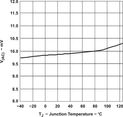
TPS2410 TPS2411 regv_v_tj_lvs727.gifFigure 1. TPS2410 V(AC) Regulation Voltage vs Temperature
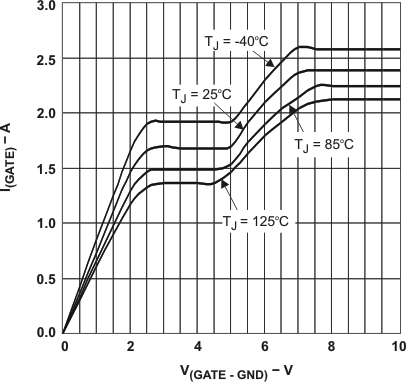
TPS2410 TPS2411 pulse_v_gatev_lvs727.gifFigure 3. Pulsed Gate Sinking Current vs Gate Voltage
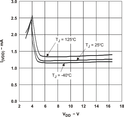
TPS2410 TPS2411 idd_v_vdd_lvs727.gifFigure 5. VDD Current vs VDD Voltage
(Gate Saturated High)
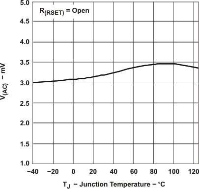
TPS2410 TPS2411 toff_v_tj_lvs727.gifFigure 2. Fast Turnoff Threshold vs Temperature
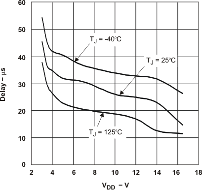
TPS2410 TPS2411 ton_v_vdd_lvs727.gifFigure 4. Turnon Delay vs VDD
(Power Applied Until Gate Is Active)