SLVS763E June 2007 – July 2015 TPS62260 , TPS62261 , TPS62262 , TPS62263
PRODUCTION DATA.
- 1 Features
- 2 Applications
- 3 Description
- 4 Revision History
- 5 Device Comparison Table
- 6 Pin Configuration and Functions
- 7 Specifications
- 8 Detailed Description
- 9 Application and Implementation
- 10Power Supply Recommendations
- 11Layout
- 12Device and Documentation Support
- 13Mechanical, Packaging, and Orderable Information
9 Application and Implementation
NOTE
Information in the following applications sections is not part of the TI component specification, and TI does not warrant its accuracy or completeness. TI’s customers are responsible for determining suitability of components for their purposes. Customers should validate and test their design implementation to confirm system functionality.
9.1 Application Information
The TPS6226x device is a high-efficiency synchronous step-down DC/DC converter featuring power save mode or 2.25 MHz fixed frequency operation.
9.2 Typical Application
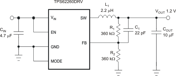 Figure 6. TPS62260DRV Adjustable 1.2-V Output
9.2.1 Design Requirements
The device operates over an input voltage range from 2 V to 6 V. The output voltage is adjustable using an external feedback divider.
9.2.2 Detailed Design Procedure
Table 1. List of Components
| COMPONENT REFERENCE | PART NUMBER | MANUFACTURER | VALUE |
|---|---|---|---|
| CIN | GRM188R60J475K | Murata | 4.7 μF, 6.3 V. X5R Ceramic |
| COUT | GRM188R60J106M | Murata | 10 μF, 6.3 V. X5R Ceramic |
| C1 | Murata | 22 pF, COG Ceramic | |
| L1 | LPS3015 | Coilcraft | 2.2 μH, 110 mΩ |
| R1, R2 | Values depending on the programmed output voltage | ||
9.2.2.1 Output Voltage Setting
The output voltage can be calculated to:
 with an internal reference voltage VREF typical 0.6 V.
To minimize the current through the feedback divider network, R2 should be 180 kΩ or 360 kΩ. The sum of R1 and R2 should not exceed ~1 MΩ, to keep the network robust against noise.
An external feed forward capacitor C1 is required for optimum load transient response. The value of C1 should be in the range between 22 pF and 33 pF.
Route the FB line away from noise sources, such as the inductor or the SW line.
9.2.2.2 Output Filter Design (Inductor and Output Capacitor)
The TPS6226x is designed to operate with inductors in the range of 1.5 μH to 4.7 μH and with output capacitors in the range of 4.7 μF to 22 μF. The part is optimized for operation with a 2.2-μH inductor and 10-μF output capacitor.
Larger or smaller inductor values can be used to optimize the performance of the device for specific operation conditions. For stable operation, the L and C values of the output filter may not fall below 1-μH effective inductance and 3.5-μF effective capacitance.
Selecting larger capacitors is less critical because the corner frequency of the L-C filter moves to lower frequencies with fewer stability problems.
9.2.2.2.1 Inductor Selection
The inductor value has a direct effect on the ripple current. The selected inductor has to be rated for its DC resistance and saturation current. The inductor ripple current (ΔIL) decreases with higher inductance and increases with higher VIN or VOUT.
The inductor selection also has an impact on the output voltage ripple in the PFM mode. Higher inductor values will lead to lower output voltage ripple and higher PFM frequency, lower inductor values will lead to a higher output voltage ripple but lower PFM frequency.
Equation 2 calculates the maximum inductor current in PWM mode under static load conditions. The saturation current of the inductor should be rated higher than the maximum inductor current as calculated with Equation 3. This is recommended because during heavy load transient the inductor current will rise above the calculated value.

where
- f = Switching frequency (2.25-MHz typical)
- L = Inductor value
- ΔIL = Peak-to-peak inductor ripple current

where
- ΔIL = Peak-to-peak inductor ripple current
- ILmax = Maximum inductor current
A more conservative approach is to select the inductor current rating just for the maximum switch current limit ILIMF of the converter.
Accepting larger values of ripple current allows the use of lower inductance values, but results in higher output voltage ripple, greater core losses, and lower output current capability.
The total losses of the coil have a strong impact on the efficiency of the DC/DC conversion and consist of both the losses in the dc resistance (R(DC)) and the following frequency-dependent components:
- The losses in the core material (magnetic hysteresis loss, especially at high switching frequencies)
- Additional losses in the conductor from the skin effect (current displacement at high frequencies)
- Magnetic field losses of the neighboring windings (proximity effect)
- Radiation losses
Table 2. List of Inductors
| DIMENSIONS [mm3] | Inductance μH | INDUCTOR TYPE | SUPPLIER |
|---|---|---|---|
| 2.5 × 2.0 × 1.0 max | 2.0 | MIPS2520D2R2 | FDK |
| 2.5 × 2.0 ×1.2 max | 2.0 | MIPSA2520D2R2 | FDK |
| 2.5 × 2.0 × 1.0 max | 2.2 | KSLI-252010AG2R2 | Htachi Metals |
| 2.5 ×2.0 × 1.2 max | 2.2 | LQM2HPN2R2MJ0L | Murata |
| 3 × 3 × 1.5 max | 2.2 | LPS3015 2R2 | Coilcraft |
9.2.2.2.2 Output Capacitor Selection
The advanced fast-response voltage mode control scheme of the TPS6226x allows the use of tiny ceramic capacitors. Ceramic capacitors with low ESR values have the lowest output voltage ripple and are recommended. The output capacitor requires either an X7R or X5R dielectric. Y5V and Z5U dielectric capacitors, aside from their wide variation in capacitance over temperature, become resistive at high frequencies.
At nominal load current, the device operates in PWM mode and the RMS ripple current is calculated as:

At nominal load current, the device operates in PWM mode and the overall output voltage ripple is the sum of the voltage spike caused by the output capacitor ESR plus the voltage ripple caused by charging and discharging the output capacitor:

At light load currents, the converter operates in power save mode and the output voltage ripple is dependent on the output capacitor and inductor value. Larger output capacitor and inductor values minimize the voltage ripple in PFM mode and tighten DC output accuracy in PFM mode.
9.2.2.2.3 Input Capacitor Selection
An input capacitor is required for best input voltage filtering, and minimizing the interference with other circuits caused by high input voltage spikes. For most applications, a 4.7-μF to 10-μF ceramic capacitor is recommended. Because ceramic capacitor loses up to 80% of its initial capacitance at 5 V, it is recommended that 10-μF input capacitors be used for input voltages >4.5 V. The input capacitor can be increased without any limit for better input voltage filtering. Take care when using only small ceramic input capacitors. When a ceramic capacitor is used at the input and the power is being supplied through long wires, such as from a wall adapter, a load step at the output or VIN step on the input can induce ringing at the VIN pin. This ringing can couple to the output and be mistaken as loop instability or could even damage the part by exceeding the maximum ratings.
Table 3. List of Capacitors
| CAPACITANCE | TYPE | SIZE | SUPPLIER |
|---|---|---|---|
| 4.7 μF | GRM188R60J475K | 0603 1.6 × 0.8 × 0.8 mm3 | Murata |
| 10 μF | GRM188R60J106M69D | 0603 1.6 × 0.8 × 0.8 mm3 | Murata |
Table 1 shows the list of components for the Application Curves.
9.2.3 Application Curves
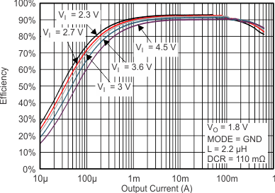 Figure 7. Efficiency (Power Save Mode) vs Output Current
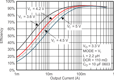 Figure 9. Efficiency (PWM Mode) vs Output Current
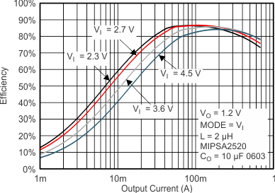 Figure 11. Efficiency vs Output Current
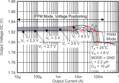 Figure 13. Output Voltage Accuracy vs Output Current
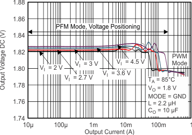 Figure 15. Output Voltage Accuracy (Power Save Mode) vs Output Current
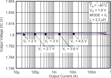 Figure 17. Output Voltage Accuracy (PWM Mode) vs Output Current
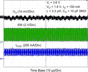 Figure 19. Typical Operation (PWM Mode)
 Figure 21. Mode Pin Transition from PFM
to Forced PWM Mode at Light Load
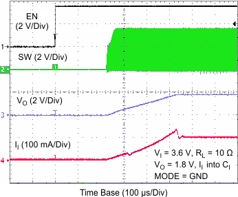 Figure 23. Start-Up Timing
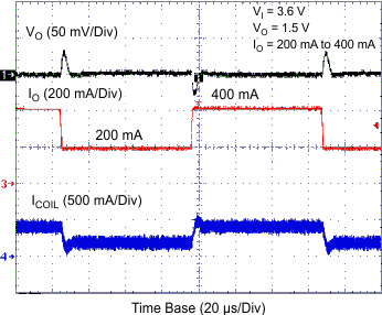 Figure 25. Load Transient (Forced PWM Mode)
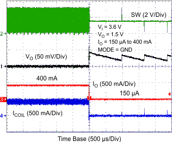 Figure 27. Load Transient (PWM Mode to PFM Mode)
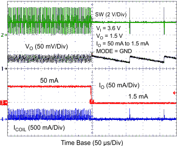 Figure 29. Load Transient (PFM Mode)
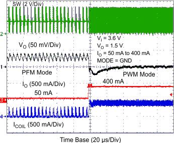 Figure 31. Load Transient (PFM Mode to PWM Mode)
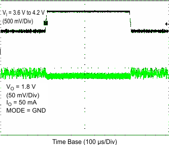 Figure 33. Line Transient (PFM Mode)
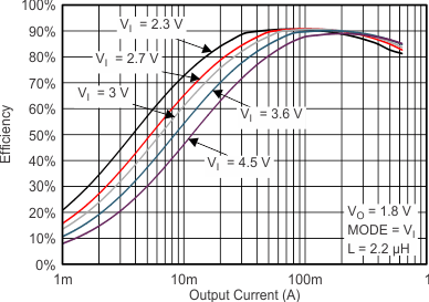 Figure 8. Efficiency (PWM Mode) vs Output Current
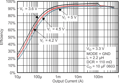 Figure 10. Efficiency (Power Save Mode) vs Output Current
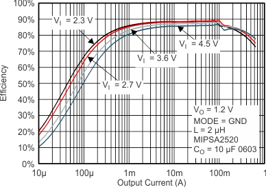 Figure 12. Efficiency vs Output Current
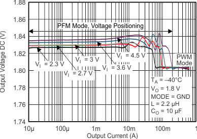 Figure 14. Output Voltage Accuracy (Power Save Mode) vs Output Current
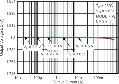 Figure 16. Output Voltage Accuracy (PWM Mode) vs Output Current
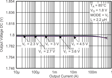 Figure 18. Output Voltage Accuracy (PWM Mode) vs Output Current
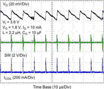 Figure 20. Typical Operation (PFM Mode)
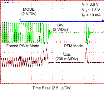 Figure 22. Mode Pin Transition from PWM
to PFM Mode at Light Load
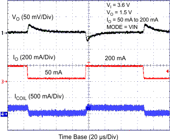 Figure 24. Load Transient (Forced PWM Mode)
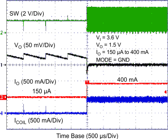 Figure 26. Load Transient (PFM Mode to PWM Mode)
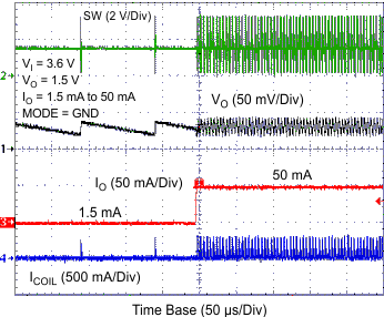 Figure 28. Load Transient (PFM Mode)
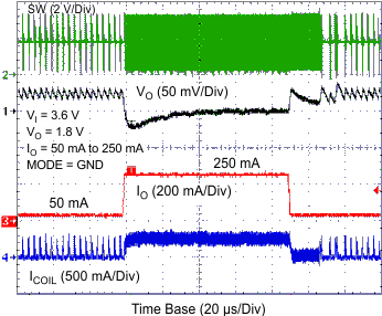 Figure 30. Load Transient (PFM Mode to PWM Mode)
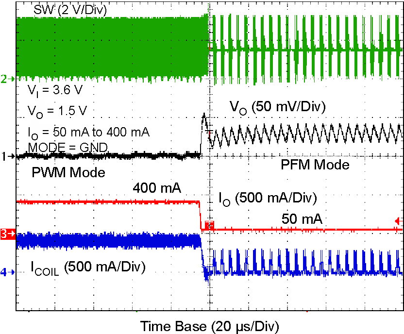 Figure 32. Load Transient (PWM Mode to PFM Mode)
 Figure 34. Line Transient (Forced PWM Mode)
9.3 System Examples
9.3.1 TPS62260, Adjustable 1.5-V Output
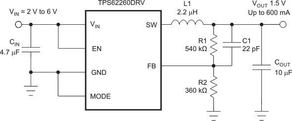 Figure 35. TPS62260 Adjustable 1.5-V Output
9.3.2 TPS62262, Fixed 1.2-V Output
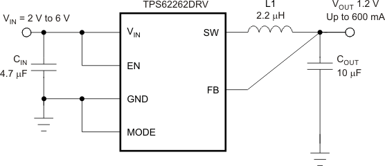 Figure 36. TPS62262 Fixed 1.2-V Output
9.3.3 TPS62261, Fixed 1.8-V Output
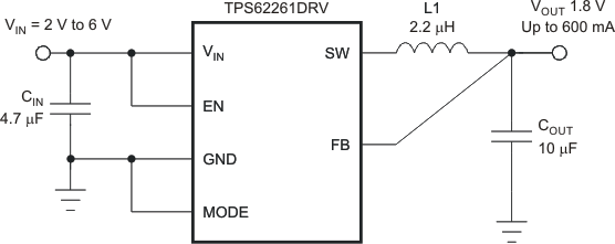 Figure 37. TPS62261 Fixed 1.8-V Output