SLVSAB2G May   2010  – December 2015 DRV8830

PRODUCTION DATA.  

  1. Features
  2. Applications
  3. Description
  4. Revision History
  5. Pin Configuration and Functions
  6. Specifications
    1. 6.1 Absolute Maximum Ratings
    2. 6.2 ESD Ratings
    3. 6.3 Recommended Operating Conditions
    4. 6.4 Thermal Information
    5. 6.5 Electrical Characteristics
    6. 6.6 I2C Timing Requirements
    7. 6.7 Typical Characteristics
  7. Detailed Description
    1. 7.1 Overview
    2. 7.2 Functional Block Diagram
    3. 7.3 Feature Description
      1. 7.3.1 Voltage Regulation
      2. 7.3.2 Voltage Setting (VSET DAC)
      3. 7.3.3 Current Limit
      4. 7.3.4 Protection Circuits
        1. 7.3.4.1 Overcurrent Protection (OCP)
        2. 7.3.4.2 Thermal Shutdown (TSD)
        3. 7.3.4.3 Undervoltage Lockout (UVLO)
    4. 7.4 Device Functional Modes
      1. 7.4.1 Bridge Control
    5. 7.5 Programming
      1. 7.5.1 I2C-Compatible Serial Interface
    6. 7.6 Register Maps
      1. 7.6.1 I2C Register Map
        1. 7.6.1.1 REGISTER 0 - CONTROL
        2. 7.6.1.2 REGISTER 1 - FAULT
  8. Application and Implementation
    1. 8.1 Application Information
    2. 8.2 Typical Application
      1. 8.2.1 Design Requirements
      2. 8.2.2 Detailed Design Procedure
        1. 8.2.2.1 Motor Voltage
        2. 8.2.2.2 Motor Current Trip Point
        3. 8.2.2.3 Sense Resistor Selection
        4. 8.2.2.4 Low Power Operation
      3. 8.2.3 Application Curves
  9. Power Supply Recommendations
    1. 9.1 Power Supervisor
    2. 9.2 Bulk Capacitance
  10. 10Layout
    1. 10.1 Layout Guidelines
    2. 10.2 Layout Example
    3. 10.3 Thermal Considerations
      1. 10.3.1 Power Dissipation
  11. 11Device and Documentation Support
    1. 11.1 Documentation Support
      1. 11.1.1 Related Documentation
    2. 11.2 Community Resources
    3. 11.3 Trademarks
    4. 11.4 Electrostatic Discharge Caution
    5. 11.5 Glossary
  12. 12Mechanical, Packaging, and Orderable Information

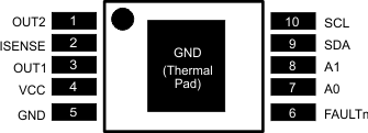
5 Pin Configuration and Functions

DGQ or DRC Package
10-Pin HVSSOP or VSON
Top View
DRV8830 po_lvsab2.gif
The HVSSOP package has a PowerPAD.

Pin Functions

PIN TYPE(1) DESCRIPTION EXTERNAL COMPONENTS
OR CONNECTIONS
NAME NO.
A0 7 I Address set 0 Connect to GND, VCC, or open to set I2C base address. See serial interface description.
A1 8 I Address set 1
FAULTn 6 OD Fault output Open-drain output driven low if fault condition present
GND 5 Device ground
ISENSE 2 IO Current sense resistor Connect current sense resistor to GND. Resistor value sets current limit level.
OUT1 3 O Bridge output 1 Connect to motor winding
OUT2 1 O Bridge output 2
SCL 10 I Serial clock Clock line of I2C serial bus
SDA 9 IO Serial data Data line of I2C serial bus
VCC 4 Device and motor supply Bypass to GND with a 0.1-μF (minimum) ceramic capacitor.
(1) Directions: I = input, O = output, OZ = tri-state output, OD = open-drain output, IO = input/output