SLVSAC3D May 2011 – December 2014 TPS62730 , TPS62732 , TPS62733
PRODUCTION DATA.
- 1 Features
- 2 Applications
- 3 Description
- 4 Revision History
- 5 Description (Continued)
- 6 Device Comparison Table
- 7 Pin Configuration and Functions
- 8 Specifications
- 9 Detailed Description
- 10Application and Implementation
- 11Power Supply Recommendations
- 12Layout
- 13Device and Documentation Support
- 14Mechanical, Packaging, and Orderable Information
7 Pin Configuration and Functions
DRY Package
6 Pins
Top View
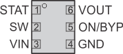
Pin Functions
| PIN | I/O | DESCRIPTION | |
|---|---|---|---|
| NAME | NO | ||
| VIN | 3 | PWR | VIN power supply pin. Connect this pin close to the VIN terminal of the input capacitor. A ceramic capacitor of 2.2 µF is required. |
| GND | 4 | PWR | GND supply pin. Connect this pin close to the GND terminal of the input and output capacitor. |
| ON/BYP | 5 | IN | This is the mode selection pin of the device. Pulling this pin to low forces the device into ultra low-power bypass mode. The output of the DC-DC converter is connected to VIN through an internal bypass switch. Pulling this pin to high enables the DC-DC converter operation. This pin must be terminated and is controlled by the system. |
| SW | 2 | OUT | This is the switch pin and is connected to the internal MOSFET switches. Connect the inductor to this terminal. |
| VOUT | 6 | IN | Feedback Pin for the internal feedback divider network and regulation loop. The internal bypass switch is connected between this pin and VIN. Connect this pin directly to the output capacitor with short trace. |
| STAT | 1 | OUT | This is the open-drain status output with active low level. An internal comparator drives this output. The pin is high impedance with ON/BYP = low. With ON/BYP set to high the device and the internal VOUT comparator becomes active. The active low STAT pin indicates if the DC-DC regulator is settled and the output voltage above the VTSTAT threshold. If not used, this pin can be left open. |