SLVSAG8G September 2011 – June 2016 TPS61253 , TPS61254 , TPS61256 , TPS61258 , TPS61259 , TPS612592
UNLESS OTHERWISE NOTED, this document contains PRODUCTION DATA.
- 1 Features
- 2 Applications
- 3 Description
- 4 Revision History
- 5 Device Options
- 6 Pin Configuration and Functions
- 7 Specifications
- 8 Parameter Measurement Information
- 9 Detailed Description
- 10Application and Implementation
- 11Power Supply Recommendations
- 12Layout
- 13Device and Documentation Support
- 14Mechanical, Packaging, and Orderable Information
10 Application and Implementation
NOTE
Information in the following applications sections is not part of the TI component specification, and TI does not warrant its accuracy or completeness. TI’s customers are responsible for determining suitability of components for their purposes. Customers should validate and test their design implementation to confirm system functionality.
10.1 Application Information
With a wide input voltage range of 2.3 V to 5.5 V, the TPS6125x supports applications powered by Li-Ion batteries with extended voltage range. Intended for low-power applications, it supports up to 800-mA load current from a battery discharged as low as 2.65 V and allows the use of low cost chip inductor and capacitors. Different fixed voltage output versions are available from 3.15 V to 5.0 V. The TPS6125x offers a very small solution size due to minimum amount of external components. It allows the use of small inductors and input capacitors to achieve a small solution size. During shutdown, the load is completely disconnected from the battery.
10.2 Typical Application
This section details an application with TPS61256 to output fixed 5.0 V.
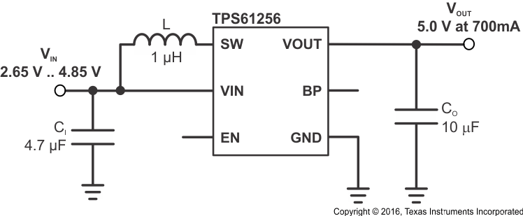 Figure 28. Smallest Solution Size Application
10.2.1 Design Requirements
In this example, TPS61256 is used to design a 5-V power supply with up to 700-mA output current capability. The TPS61256 can be powered by one-cell Li-ion battery, and in this example the input voltage range is from 2.65 V to 4.85 V.
10.2.2 Detailed Design Procedure
Table 3. List of Components
| REFERENCE | DESCRIPTION | PART NUMBER, MANUFACTURER(1) |
|---|---|---|
| L(2) | 1.0 μH, 1.8 A, 48 mΩ, 3.2 x 2.5 x 1.0mm max. height | LQM32PN1R0MG0, muRata |
| L(3) | 1.0 μH, 3.7 A, 37 mΩ, 3.2 x 2.5 x 1.2mm max. height | DFE322512C, TOKO |
| CI | 4.7 μF, 6.3 V, 0402, X5R ceramic | GRM155R60J475M, muRata |
| CO | 10 μF, 6.3 V, 0603, X5R ceramic | GRM188R60J106ME84, muRata |
10.2.2.1 Inductor Selection
A boost converter normally requires two main passive components for storing energy during the conversion, an inductor and an output capacitor. It is advisable to select an inductor with a saturation current rating higher than the possible peak current flowing through the power switches.
The inductor peak current varies as a function of the load, the input and output voltages and can be estimated using Equation 4.

Selecting an inductor with insufficient saturation performance can lead to excessive peak current in the converter. This could eventually harm the device and reduce its reliability.
When selecting the inductor, as well as the inductance, parameters of importance are: maximum current rating, series resistance, and operating temperature. The inductor DC current rating should be greater (by some margin) than the maximum input average current, refer to Equation 5 and Current Limit Operation section for more details.

The TPS6125x series of step-up converters have been optimized to operate with a effective inductance in the range of 0.7 µH to 2.9 µH and with output capacitors in the range of 10 µF to 47 µF. The internal compensation is optimized for an output filter of L = 1 µH and CO = 10 µF. Larger or smaller inductor values can be used to optimize the performance of the device for specific operating conditions. For more details, see the Checking Loop Stability section.
In high-frequency converter applications, the efficiency is essentially affected by the inductor AC resistance (i.e. quality factor) and to a smaller extent by the inductor DCR value. To achieve high efficiency operation, care should be taken in selecting inductors featuring a quality factor above 25 at the switching frequency. Increasing the inductor value produces lower RMS currents, but degrades transient response. For a given physical inductor size, increased inductance usually results in an inductor with lower saturation current.
The total losses of the coil consist of both the losses in the DC resistance, R(DC) , and the following frequency-dependent components:
- The losses in the core material (magnetic hysteresis loss, especially at high switching frequencies)
- Additional losses in the conductor from the skin effect (current displacement at high frequencies)
- Magnetic field losses of the neighboring windings (proximity effect)
- Radiation losses
The following inductor series from different suppliers have been used with the TPS6125x converters.
Table 4. List of Inductors
| MANUFACTURER(1) | SERIES | DIMENSIONS (in mm) |
|---|---|---|
| HITACHI METALS | KSLI-322512BL1-1R0 | 3.2 x 2.5 x 1.2 max. height |
| MURATA | LQM32PN1R0MG0 | 3.2 x 2.5 x 1.0 max. height |
| LQM2HPN1R0MG0 | 2.5 x 2.0 x 1.0 max. height | |
| LQM21PN1R5MC0 | 2.0 x 1.2 x 0.55 max height | |
| TOKO | DFE322512C-1R0 | 3.2 x 2.5 x 1.2 max. height |
| MDT2012-CLR1R0AM | 2.0 x 1.2 x 0.58 max height |
10.2.2.2 Output Capacitor
For the output capacitor, it is recommended to use small ceramic capacitors placed as close as possible to the VOUT and GND pins of the IC. If, for any reason, the application requires the use of large capacitors which can not be placed close to the IC, using a smaller ceramic capacitor in parallel to the large one is highly recommended. This small capacitor should be placed as close as possible to the VOUT and GND pins of the IC. To get an estimate of the recommended minimum output capacitance, Equation 6 can be used.

Where f is the switching frequency which is 3.5 MHz (typ.) and ΔV is the maximum allowed output ripple.
With a chosen ripple voltage of 20mV, a minimum effective capacitance of 9μF is needed. The total ripple is larger due to the ESR of the output capacitor. This additional component of the ripple can be calculated using Equation 7

An MLCC capacitor with twice the value of the calculated minimum should be used due to DC bias effects. This is required to maintain control loop stability. The output capacitor requires either an X7R or X5R dielectric. Y5V and Z5U dielectric capacitors, aside from their wide variation in capacitance over temperature, become resistive at high frequencies. There are no additional requirements regarding minimum ESR. Larger capacitors cause lower output voltage ripple as well as lower output voltage drop during load transients but the total output capacitance value should not exceed ca. 50µF.
DC bias effect: high cap. ceramic capacitors exhibit DC bias effects, which have a strong influence on the device's effective capacitance. Therefore the right capacitor value has to be chosen very carefully. Package size and voltage rating in combination with material are responsible for differences between the rated capacitor value and it's effective capacitance. For instance, a 10-µF X5R 6.3-V 0603 MLCC capacitor would typically show an effective capacitance of less than 4 µF (under 5 V bias condition, high temperature).
In applications featuring high pulsed load currents (e.g. TPS61253 based solution) it is recommended to run the converter with a reasonable amount of effective output capacitance, for instance x2 10-µF X5R 6.3-V 0603 MLCC capacitors connected in parallel.
10.2.2.3 Input Capacitor
Multilayer ceramic capacitors are an excellent choice for input decoupling of the step-up converter as they have extremely low ESR and are available in small footprints. Input capacitors should be located as close as possible to the device. While a 4.7-μF input capacitor is sufficient for most applications, larger values may be used to reduce input current ripple without limitations.
Take care when using only ceramic input capacitors. When a ceramic capacitor is used at the input and the power is being supplied through long wires, such as from a wall adapter, a load step at the output can induce ringing at the VIN pin. This ringing can couple to the output and be mistaken as loop instability or could even damage the part. Additional "bulk" capacitance (electrolytic or tantalum) should in this circumstance be placed between CI and the power source lead to reduce ringing that can occur between the inductance of the power source leads and CI.
10.2.2.4 Checking Loop Stability
The first step of circuit and stability evaluation is to look from a steady-state perspective at the following signals:
- Switching node, SW
- Inductor current, IL
- Output ripple voltage, VOUT(AC)
These are the basic signals that need to be measured when evaluating a switching converter. When the switching waveform shows large duty cycle jitter or the output voltage or inductor current shows oscillations, the regulation loop may be unstable. This is often a result of board layout and/or L-C combination.
As a next step in the evaluation of the regulation loop, the load transient response is tested. The time between the application of the load transient and the turn on of the P-channel MOSFET, the output capacitor must supply all of the current required by the load. VOUT immediately shifts by an amount equal to ΔI(LOAD) x ESR, where ESR is the effective series resistance of COUT. ΔI(LOAD) begins to charge or discharge COUT generating a feedback error signal used by the regulator to return VOUT to its steady-state value. The results are most easily interpreted when the device operates in PWM mode.
During this recovery time, VOUT can be monitored for settling time, overshoot or ringing that helps judge the converter’s stability. Without any ringing, the loop has usually more than 45° of phase margin. Because the damping factor of the circuitry is directly related to several resistive parameters (e.g., MOSFET rDS(on)) that are temperature dependant, the loop stability analysis has to be done over the input voltage range, load current range, and temperature range.
10.2.3 Application Curves
| FIGURE | |
|---|---|
| PFM operation | Figure 29 |
| PWM operation | Figure 30 |
| Combined line/load transient response | Figure 31 |
| Load transient response | Figure 32, Figure 34 |
| AC load transient response | Figure 33, Figure 35 |
| Start-up | Figure 36, Figure 37 |
spacing
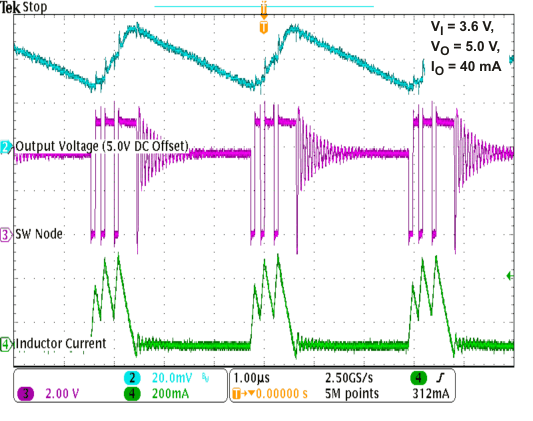 Figure 29. Power-Save Mode Operation
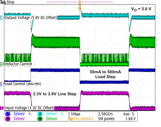 Figure 31. Combined Line/Load Transient Response
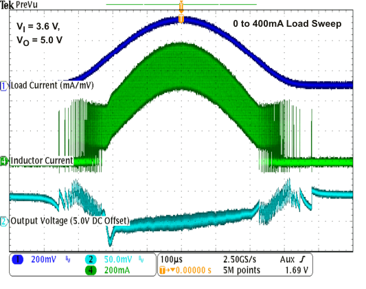 Figure 33. AC Load Transient Response
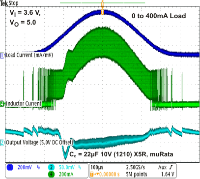
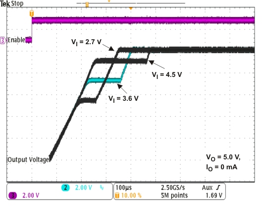 Figure 37. Start-Up
 Figure 30. PWM Operation
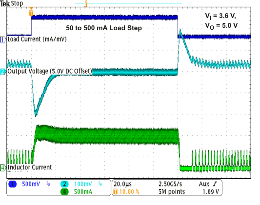 Figure 32. Load Transient Response in PFM/PWM Operation
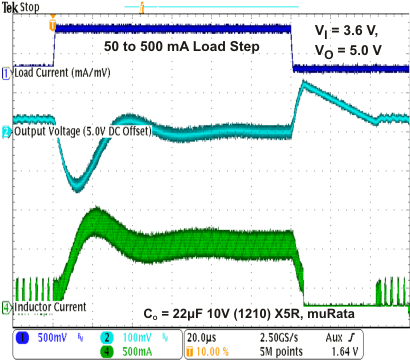
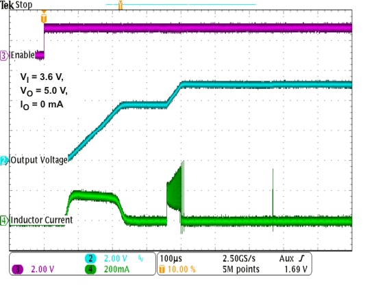 Figure 36. Start-Up
10.3 System Examples
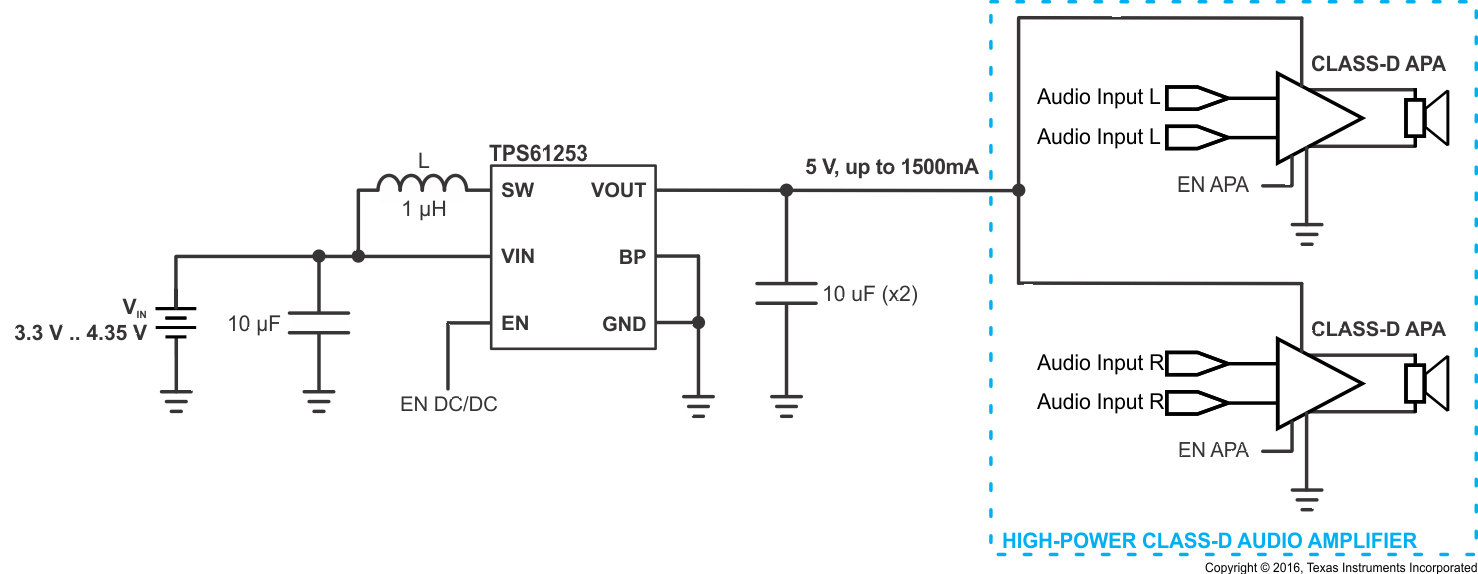 Figure 38. "Boosted" Stereo Audio Power Supply
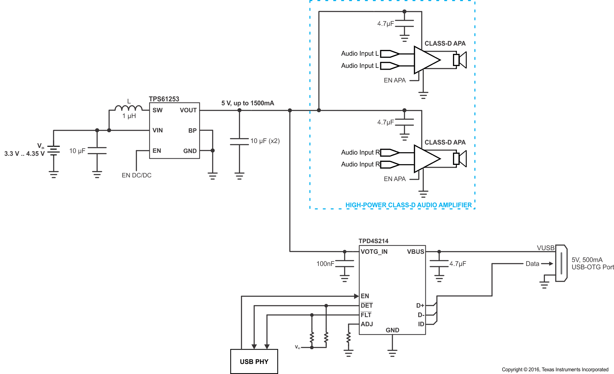 Figure 39. Single Cell Li-Ion Power Solution for Tablet PCs Featuring
"Boosted" Audio Power Supply and USB-OTG I/F
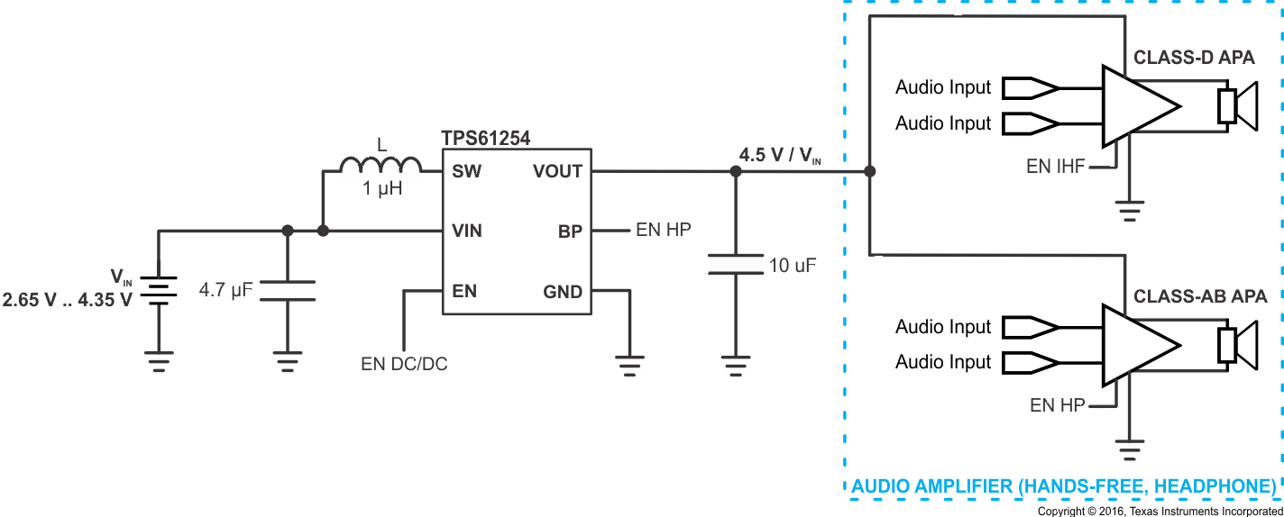 Figure 40. Combined Audio Amplifier Power Supply
 Figure 41. "Boosted" Audio Power Supply
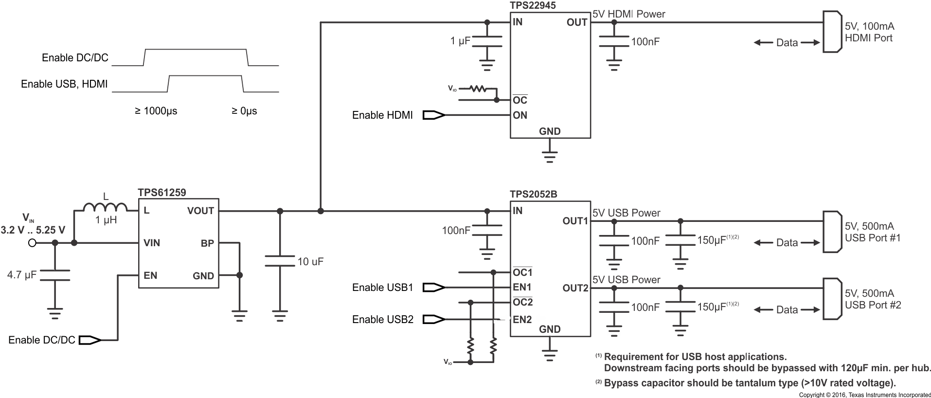 Figure 42. Single Cell Li-Ion Power Solution for Tablet PCs Featuring x2 USB Host Ports, HDMI I/F