SLVSAW2C March 2012 – October 2016 TPS62090 , TPS62091 , TPS62092 , TPS62093
PRODUCTION DATA.
- 1 Features
- 2 Applications
- 3 Description
- 4 Revision History
- 5 Device Comparison Table
- 6 Pin Configuration and Functions
- 7 Specifications
-
8 Detailed Description
- 8.1 Overview
- 8.2 Functional Block Diagram
- 8.3
Feature Description
- 8.3.1 Enable and Disable (EN)
- 8.3.2 Softstart (SS) and Hiccup Current Limit During Startup
- 8.3.3 Voltage Tracking (SS)
- 8.3.4 Short Circuit Protection (Hiccup-Mode)
- 8.3.5 Output Discharge Function
- 8.3.6 Power Good Output (PG)
- 8.3.7 Frequency Set Pin (FREQ)
- 8.3.8 Undervoltage Lockout (UVLO)
- 8.3.9 Thermal Shutdown
- 8.3.10 Charge Pump (CP, CN)
- 8.4 Device Functional Modes
- 9 Application and Implementation
- 10Power Supply Recommendations
- 11Layout
- 12Device and Documentation Support
- 13Mechanical, Packaging, and Orderable Information
9 Application and Implementation
NOTE
Information in the following applications sections is not part of the TI component specification, and TI does not warrant its accuracy or completeness. TI’s customers are responsible for determining suitability of components for their purposes. Customers should validate and test their design implementation to confirm system functionality.
9.1 Application Information
The TPS6209x 3 A family of devices, are high frequency synchronous step down converters optimized for small solution size, high efficiency and suitable for battery powered applications.
9.2 Typical Applications
9.2.1 Design Requirements
The design guideline provides a component selection to operate the device within the recommended operating conditions.
The design can be optimized for highest efficiency or smallest solution size and lowest output voltage ripple. For highest efficiency set the device switching frequency to 1.4 MHz (FREQ = High) and select the output filter components according to Table 3. For smallest solution size and lowest output voltage ripple set the device switching frequency to 2.8 MHz (FREQ = Low) and select the output filter components according to Table 2. For the fixed output voltage option the feedback pin needs to be connected to GND.
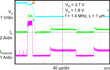
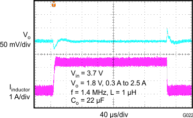
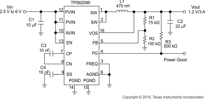
Table 1 shows the list of components for the Application Curves.
Table 1. List of Components
| REFERENCE | DESCRIPTION | MANUFACTURER |
|---|---|---|
| TPS62090 | High efficiency step down converter | Texas Instruments |
| L1 | Inductor: 1uH, 0.47uH, 0.4uH | Coilcraft XFL4020-102, TOKO DEF252012C-R47, Coilcraft XAL4020-401 |
| C1 | Ceramic capacitor: 10uF, 22uF | (6.3V, X5R, 0603), (6.3V, X5R, 0805) |
| C2 | Ceramic capacitor: 22uF | (6.3V, X5R, 0805) |
| C3, C4 | Ceramic capacitor | Standard |
| R1, R2, R3 | Resistor | Standard |
9.2.2 Detailed Design Procedure
The first step is the selection of the output filter components. To simplify this process, Table 2 and Table 3 outline possible inductor and capacitor value combinations. Checked cells represent combinations that are proven for stability by simulation and lab. Further combinations should be checked for each individual application.
Table 2. Output Filter Selection (2.8 MHz Operation, FREQ = GND)
| INDUCTOR VALUE [µH](3) | OUTPUT CAPACITOR VALUE [µF](2) | ||||
|---|---|---|---|---|---|
| 10 | 22 | 47 | 100 | 150 | |
| 0.47 | √(1) | √ | √ | √ | |
| 1.0 | √ | √ | √ | √ | √ |
| 2.2 | |||||
| 3.3 | |||||
Table 3. Output Filter Selection (1.4 MHz Operation, FREQ = VIN)
| INDUCTOR VALUE [µH](3) | OUTPUT CAPACITOR VALUE [µF](2) | ||||
|---|---|---|---|---|---|
| 10 | 22 | 47 | 100 | 150 | |
| 0.47 | √ | √ | √ | √ | |
| 1.0 | √ | √(1) | √ | √ | √ |
| 2.2 | √ | √ | √ | √ | √ |
| 3.3 | |||||
9.2.2.1 Inductor Selection
The inductor selection is affected by several parameter like inductor ripple current, output voltage ripple, transition point into power save mode, and efficiency. See Table 4 for typical inductors.
Table 4. Inductor Selection
| INDUCTOR VALUE | COMPONENT SUPPLIER(1) | SIZE (LxWxH mm) | Isat/DCR |
|---|---|---|---|
| 0.6 µH | Coilcraft XAL4012-601 | 4 x 4 x 2.1 | 7.1 A/9.5 mΩ |
| 1 µH | Coilcraft XAL4020-102 | 4 x 4 x 2.1 | 5.9 A/13.2 mΩ |
| 1 µH | Coilcraft XFL4020-102 | 4 x 4 x 2.1 | 5.1 A/10.8 mΩ |
| 0.47 µH | TOKO DFE252012 R47 | 2.5 x 2 x 1.2 | 3.7 A/39 mΩ |
| 1 µH | TOKO DFE252012 1R0 | 2.5 x 2 x 1.2 | 3.0 A/59 mΩ |
| 0.68 µH | TOKO DFE322512 R68 | 3.2 x 2.5 x 1.2 | 3.5 A/37 mΩ |
| 1 µH | TOKO DFE322512 1R0 | 3.2 x 2.5 x 1.2 | 3.1 A/45 mΩ |
In addition, the inductor has to be rated for the appropriate saturation current and DC resistance (DCR). Equation 6 calculates the maximum inductor current under static load conditions. The formula takes the converter efficiency into account. The converter efficiency can be taken from the data sheet graph`s or 80% can be used as a conservative approach. The calculation must be done for the maximum input voltage where the peak switch current is highest.


where
- ƒ = Converter switching frequency (typical 2.8 MHz or 1.4 MHz)
- L = Selected inductor value
- η = Estimated converter efficiency (use the number from the efficiency curves or 0.80 as an conservative assumption)
Note: The calculation must be done for the maximum input voltage of the application
Calculating the maximum inductor current using the actual operating conditions gives the minimum saturation current. A margin of 20% needs to be added to cover for load transients during operation.
9.2.2.2 Input and Output Capacitor Selection
For best output and input voltage filtering, low ESR (X5R or X7R) ceramic capacitors are recommended. The input capacitor minimizes input voltage ripple, suppresses input voltage spikes and provides a stable system rail for the device. A 10-μF or larger input capacitor is recommended when FREQ = Low and a 22-uF or larger when FREQ = High.
The output capacitor value can range from 10 μF up to 150 μF and beyond. Load transient testing and measuring the bode plot are good ways to verify stability with larger capacitor values. The recommended typical output capacitor value is 22 μF (nominal) and can vary over a wide range as outline in the output filter selection table. For output voltages above 1.8 V, noise can cause duty cycle jitter. This does not degrade device performance. Using an output capacitor of 2 x 22 μF (nominal) for output voltages >1.8 V avoids duty cycle jitter.
Ceramic capacitor have a DC-Bias effect, which has a strong influence on the final effective capacitance. Choose the right capacitor carefully in combination with considering its package size and voltage rating.
9.2.2.3 Setting the Output Voltage
The output voltage is set by an external resistor divider according to the following equations:


When sizing R2, in order to achieve low quiescent current and acceptable noise sensitivity, use a minimum of 5 µA for the feedback current IFB. Larger currents through R2 improve noise sensitivity and output voltage accuracy. Lowest current consumption and best output voltage accuracy can be achieved with the fixed output voltage versions. For the fixed output voltage versions, the FB pin can be left floating or connected to GND to improve the thermal performance. A feed forward capacitor is not required for proper operation.
9.2.2.4 Application Curves
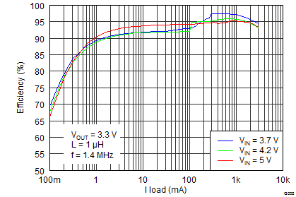
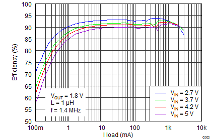
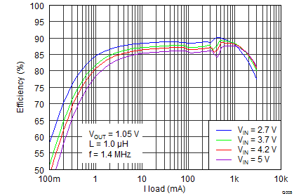
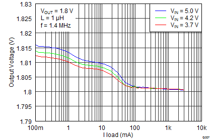
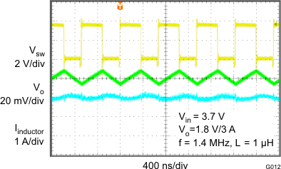
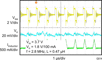
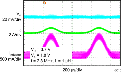
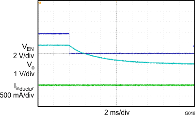
| VO = 1.8 V / No Load | f = 1.4 MHz / L = 1µH |
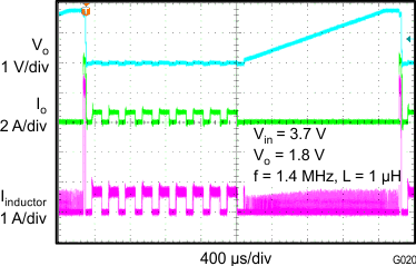
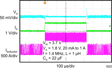
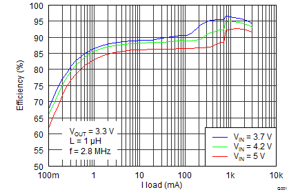
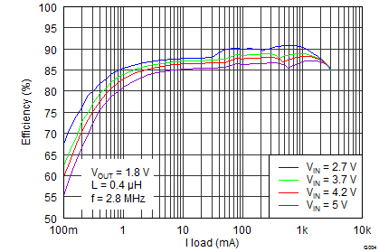
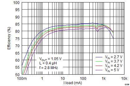
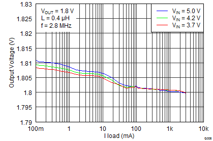
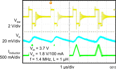
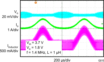
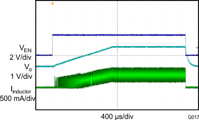
| VO = 1.8 V / 600mA | f = 2.8 MHz / L = 1µH | CSS = 10 nF |
