SLVSB09C September 2011 – October 2017 TPS54623
PRODUCTION DATA.
- 1 Features
- 2 Applications
- 3 Description
- 4 Revision History
- 5 Pin Configuration and Functions
- 6 Specifications
-
7 Detailed Description
- 7.1 Overview
- 7.2 Functional Block Diagram
- 7.3
Feature Description
- 7.3.1 VIN and Power VIN Pins (VIN and PVIN)
- 7.3.2 Voltage Reference
- 7.3.3 Adjusting the Output Voltage
- 7.3.4 Safe Start-up into Pre-Biased Outputs
- 7.3.5 Error Amplifier
- 7.3.6 Slope Compensation
- 7.3.7 Enable and Adjusting Undervoltage Lockout
- 7.3.8 Slow Start (SS/TR)
- 7.3.9 Power Good (PWRGD)
- 7.3.10 Bootstrap Voltage (BOOT) and Low Dropout Operation
- 7.3.11 Sequencing (SS/TR)
- 7.3.12 Output Overvoltage Protection (OVP)
- 7.3.13 Overcurrent Protection
- 7.3.14 Thermal Shutdown
- 7.3.15 Small Signal Model for Loop Response
- 7.3.16 Simple Small Signal Model for Peak Current Mode Control
- 7.3.17 Small Signal Model for Frequency Compensation
- 7.4 Device Functional Modes
-
8 Application and Implementation
- 8.1 Application Information
- 8.2
Typical Application
- 8.2.1 Design Requirements
- 8.2.2
Detailed Design Procedure
- 8.2.2.1 Custom Design With WEBENCH® Tools
- 8.2.2.2 Operating Frequency
- 8.2.2.3 Output Inductor Selection
- 8.2.2.4 Output Capacitor Selection
- 8.2.2.5 Input Capacitor Selection
- 8.2.2.6 Slow Start Capacitor Selection
- 8.2.2.7 Bootstrap Capacitor Selection
- 8.2.2.8 Under Voltage Lockout Set Point
- 8.2.2.9 Output Voltage Feedback Resistor Selection
- 8.2.2.10 Compensation Component Selection
- 8.2.3 Application Curves
- 9 Power Supply Recommendations
- 10Layout
- 11Device and Documentation Support
- 12Mechanical, Packaging, and Orderable Information
1 Features
- Integrated 26 mΩ, 19 mΩ MOSFETs
- Split Power Rail: 1.6 V to 17 V on PVIN
- 200 kHz to 1.6 MHz Switching Frequency
- Light Load Efficient With Pulse Skip
- Synchronizes to External Clock
- 0.6 V ±1% Voltage Reference Overtemperature
- Low 2-µA Shutdown Quiescent Current
- Monotonic Start-Up into Pre-biased Outputs
- –40°C to 150°C Operating Junction Temperature Range
- Adjustable Slow Start and Power Sequencing
- Power Good Output Monitor for Undervoltage and Overvoltage
- Adjustable Input Undervoltage Lockout
- Create a Custom Design Using the TPS54623 With the WEBENCH® Power Designer
2 Applications
- High Density Distributed Power Systems
- High Performance Point of Load Regulation
- Broadband, Networking, and Optical Communications Infrastructure
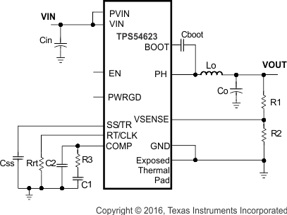
Simplified Schematic

3 Description
The TPS54623 in thermally enhanced VQFN package is a full featured 17-V, 6-A synchronous step-down converter which is optimized for small designs through high efficiency and integrating the high-side and low-side MOSFETs. Further space savings are achieved through current mode control, which reduces component count, and by selecting a high switching frequency, reducing the inductor's footprint.
The output voltage start-up ramp is controlled by the SS/TR pin, which allows operation as either a stand alone power supply or in tracking situations. Power sequencing is also possible by correctly configuring the enable and the open drain power good pins.
Cycle-by-cycle current limiting on the high-side FET protects the device in overload situations and is enhanced by a low-side sourcing current limit which prevents current runaway. There is also a low-side sinking current limit that turns off the low-side MOSFET to prevent excessive reverse current. Hiccup protection will be triggered if the overcurrent condition has persisted for longer than the preset time. Thermal hiccup protection disables the device when the die temperature exceeds the thermal shutdown temperature and enables the part again after the built-in thermal shutdown hiccup time. The TPS54623 operates at continuous current mode (CCM) at higher load conditions while skipping pulses to boost the efficiency at light loads.
Device Information(1)
| PART NUMBER | PACKAGE | BODY SIZE (NOM) |
|---|---|---|
| TPS54623 | VQFN (14) | 3.50 mm × 3.50 mm |
- For all available packages, see the orderable addendum at the end of the data sheet.
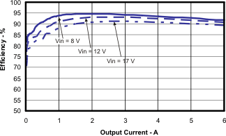
Efficiency vs Load Current

4 Revision History
Changes from B Revision (January 2017) to C Revision
- Added top nav icon for TI Design Go
- Added links for WEBENCH on page 1 and in Application and Implementation and Device and Documentation Support sections Go
- minor editorial edits Go
- Changed RθJA value from "47.2" to "40.1" Go
- Changed RθJCtop value from "64.8" to "34.4" Go
- RθJB value from "14.4" to "11.4" Go
- Changed ψJB value from "14.7" to "11.4" Go
- Changed RθJCbot value from "3.2" to "1.8" Go
- Added new paragraph to end of Sequencing (SS/TR) Go
Changes from A Revision (March 2016) to B Revision
- Changed Error amplifier dc gain test conditions, VSENSE from 0.8 V to 0.6 V Go
- Changed the voltage reference (Vref) from 0.8 V to 0.6 V in Slow Start (SS/TR) description. Go
- Changed "..internal voltage reference of 0.8 V. Above 0.8 V.." to "..internal voltage reference of 0.6 V. Above 0.6 V..." in Minimum Output Voltage description.Go
Changes from * Revision (September 2011) to A Revision
- Added ESD Ratings table, Feature Description section, Device Functional Modes, Application and Implementation section, Power Supply Recommendations section, Layout section, Device and Documentation Support section, and Mechanical, Packaging, and Orderable Information sectionGo
- Deleted Ordering Information tableGo