SLVSBC4G May 2012 – June 2017 TPS65381-Q1
PRODUCTION DATA.
- 1 Device Overview
- 2 Revision History
- 3 Pin Configuration and Functions
- 4 Specifications
-
5 Detailed Description
- 5.1 Overview
- 5.2 Functional Block Diagram
- 5.3 Feature Description
- 5.4
Device Functional Modes
- 5.4.1 Power-Up and Power-Down Behavior
- 5.4.2 Safety Functions and Diagnostics Overview
- 5.4.3 Voltage Monitor (VMON)
- 5.4.4 TPS65381-Q1 Internal Error Signals
- 5.4.5 Loss-of-Clock Monitor (LCMON)
- 5.4.6 Analog Built-In Self-Test (ABIST)
- 5.4.7 Logic Built-In Self-Test (LBIST)
- 5.4.8 Junction Temperature Monitoring and Current Limiting
- 5.4.9 Diagnostic MUX and Diagnostic Output Pin (DIAG_OUT)
- 5.4.10 Watchdog Timer (WD)
- 5.4.11 Watchdog Fail Counter, Status, and Fail Event
- 5.4.12 Watchdog Sequence
- 5.4.13 MCU to Watchdog Synchronization
- 5.4.14 Trigger Mode (Default Mode)
- 5.4.15 Q&A Mode
- 5.4.16 MCU Error Signal Monitor (MCU ESM)
- 5.4.17 Device Configuration Register Protection
- 5.4.18 Enable and Reset Driver Circuit
- 5.4.19 Device Operating States
- 5.4.20 STANDBY State
- 5.4.21 RESET State
- 5.4.22 DIAGNOSTIC State
- 5.4.23 ACTIVE State
- 5.4.24 SAFE State
- 5.4.25 State Transition Priorities
- 5.4.26 Power on Reset (NPOR)
- 5.5
Register Maps
- 5.5.1 Serial Peripheral Interface (SPI)
- 5.5.2 SPI Register Write Access Lock (SW_LOCK command)
- 5.5.3 SPI Registers (SPI Mapped Response)
- 5.5.4
Device Safety Status and Control Registers
- 5.5.4.1 VMON_STAT_1 Register
- 5.5.4.2 VMON_STAT_2 Register
- 5.5.4.3 SAFETY_STAT_1 Register
- 5.5.4.4 SAFETY_STAT_2 Register
- 5.5.4.5 SAFETY_STAT_3 Register
- 5.5.4.6 SAFETY_STAT_4 Register
- 5.5.4.7 SAFETY_STAT_5 Register
- 5.5.4.8 SAFETY_ERR_CFG Register
- 5.5.4.9 SAFETY_BIST_CTRL Register
- 5.5.4.10 SAFETY_CHECK_CTRL Register
- 5.5.4.11 SAFETY_FUNC_CFG Register
- 5.5.4.12 SAFETY_ERR_STAT Register
- 5.5.4.13 SAFETY_ERR_PWM_H Register
- 5.5.4.14 SAFETY_ERR_PWM_L Register
- 5.5.4.15 SAFETY_PWD_THR_CFG Register
- 5.5.4.16 SAFETY_CFG_CRC Register
- 5.5.4.17 Diagnostics
- 5.5.5 Watchdog Timer
- 5.5.6 Sensor Supply
-
6 Application and Implementation
- 6.1 Application Information
- 6.2
Typical Application
- 6.2.1 Design Requirements
- 6.2.2
Detailed Design Procedure
- 6.2.2.1 VDD6 Preregulator
- 6.2.2.2 VDD1 Linear Controller
- 6.2.2.3 VSOUT1 Tracking Linear Regulator, Configured to Track VDD5
- 6.2.2.4 Alternative Use for VSOUT1 Tracking Linear Regulator, Configured for 6-V Output Tracking VDD3/5 In 3.3-V Mode
- 6.2.2.5 Alternative Use for VSOUT1 Tracking Linear Regulator, Configured for 9-V Output Tracking to 5-V Input from VDD5
- 6.2.2.6 Alternative Use for VSOUT1 Tracking Linear Regulator, Configured in Non-tracking Mode Providing a 4.5-V Output
- 6.2.3 Application Curves
- 6.3 System Examples
- 7 Power Supply Recommendations
- 8 Layout
- 9 Device and Documentation Support
- 10Mechanical, Packaging, and Orderable Information
3 Pin Configuration and Functions
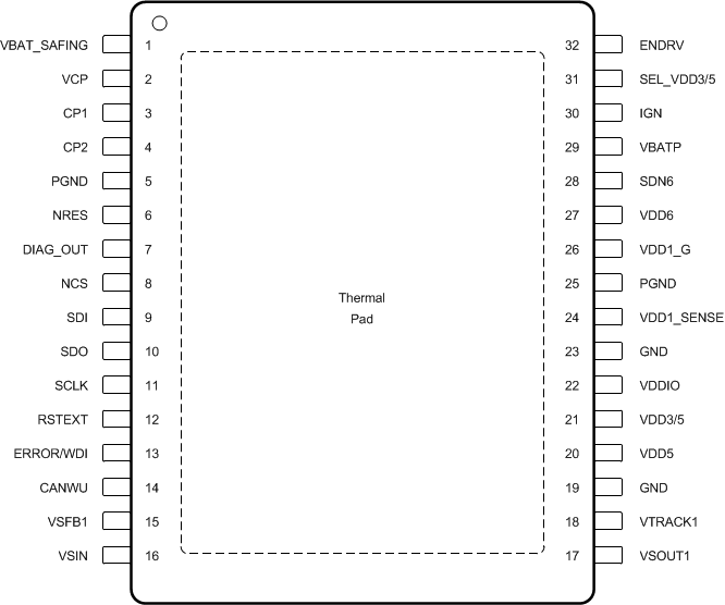
The pin configuration drawing in this section is not to scale. For package dimensions, see the mechanical data in Section 10.
DAP Package
32-Pin HTSSOP With PowerPAD™
Top View
