SLVSES3A February 2021 – March 2021 TPS62903
PRODUCTION DATA
- 1 Features
- 2 Applications
- 3 Description
- 4 Revision History
- 5 Pin Configuration and Functions
- 6 Specifications
-
7 Detailed Description
- 7.1 Overview
- 7.2 Functional Block Diagram
- 7.3
Feature Description
- 7.3.1 Mode Selection and Device Configuration MODE/S-CONF
- 7.3.2 Adjustable VO Operation (External Voltage Divider)
- 7.3.3 Setable VO Operation (VSET and Internal Voltage Divider)
- 7.3.4 Soft Start / Tracking (SS/TR)
- 7.3.5 Smart Enable with Precise Threshold
- 7.3.6 Power Good (PG)
- 7.3.7 Undervoltage Lockout (UVLO)
- 7.3.8 Current Limit And Short Circuit Protection
- 7.3.9 Thermal Shutdown
- 7.4 Device Functional Modes
-
8 Application and Implementation
- 8.1 Application Information
- 8.2
Typical Application with Adjustable Output Voltage
- 8.2.1 Design Requirements
- 8.2.2 Detailed Design Procedure
- 8.2.3 Application Curves
- 8.2.4 Typical Application with Setable VO using VSET
- 8.3 System Examples
- 9 Power Supply Recommendations
- 10Layout
- 11Device and Documentation Support
- 12Mechanical, Packaging, and Orderable Information
7.3.3 Setable VO Operation (VSET and Internal Voltage Divider)
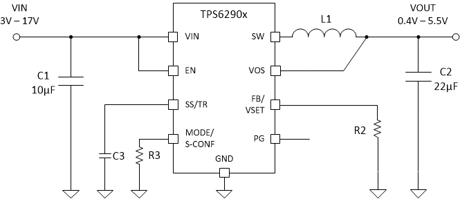
If the device is configured to VSET-operation, VO is sensed only through the VOS pin by an internal resistor divider. The target VO is programmed by an external resitor connected between the VSET pin and GND. Figure 7-3 shows the typical schematic for this configuration.
 Figure 7-3 Setable VO Operation
Schematic
Figure 7-3 Setable VO Operation
SchematicTable 7-2 VSET Selection Table
| # | RESISTOR VALUE [Ω] | TARGET VO [V] |
|---|---|---|
| 1 | GND | 1.2 |
| 2 | 4.64 k | 0.4 |
| 3 | 5.76 k | 0.6 |
| 4 | 7.15 k | 0.8 |
| 5 | 8.87 k | 1.0 |
| 6 | 11.0 k | 1.1 |
| 7 | 13.7 k | 1.3 |
| 8 | 16.9 k | 1.35 |
| 9 | 21.0 k | 1.8 |
| 10 | 26.1 k | 1.9 |
| 11 | 40.2 k | 2.5 |
| 12 | 61.9 k | 3.8 |
| 13 | 76.8 k | 5.0 |
| 14 | 95.3 k | 5.1 |
| 15 | 118.0 k | 5.5 |
| 16 | 249.00 k or larger/Open | 3.3 |