SLVSF24C december 2020 – may 2023 TPS272C45
PRODUCTION DATA
- 1
- 1 Features
- 2 Applications
- 3 Description
- 4 Revision History
- 5 Device Comparison Table
- 6 Pin Configuration and Functions
- 7 Specifications
- 8 Parameter Measurement Information
-
9 Detailed Description
- 9.1 Overview
- 9.2 Functional Block Diagram
- 9.3
Feature Description
- 9.3.1 Programmable Current Limit
- 9.3.2 Low Power Dissipation
- 9.3.3 Protection Mechanisms
- 9.3.4 Diagnostic Mechanisms
- 9.4 Device Functional Modes
- 10Application and Implementation
- 11Device and Documentation Support
- 12Mechanical, Packaging, and Orderable Information
10.2.3 Application Curves
Upon enabling our device into a capacitive load, TPS272C45 defaults the current limit to 2 times ICL for a period of time programmed set by ILIMD. In Figure 10-4, TPS272C45 charges a 1-mF capacitor using the inrush current handling feature. During the first 4 mS after enabling the device, IOUT1 is 2 times the ICL programmed (4 A). After the 4-mS period, the current folds back to the programmed ICL (2 A).
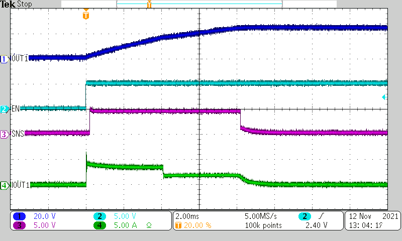 Figure 10-4 TPS272C45 Capacitor
Charging
Figure 10-4 TPS272C45 Capacitor
ChargingIf the device has a no-load case due to an open load or wire-break, the device registers the fault even in an off-state if the DIA_EN pin is high. Figure 10-5 shows the device behavior when an open load event is registered with EN low and DIAG_EN is raised. Systems can PWM DIA_EN to lower system power losses while still watching for open load events and the same timing applies.
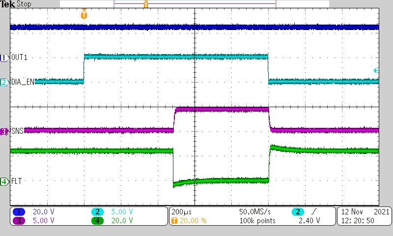 Figure 10-5 Open-Load (tOL) Detection Time
If the output of the TPS272C45 is short-circuited, the device protects the system from failure. Depending on RILIM, the current limit set-point varies. The waveforms below show examples of the current limit behavior when the device is enabled into a short circuit.
In Figure 10-6, the output is permanently shorted. Upon enabling the device, the current reaches the 2 times current limit is enabled for 6 mS set by ILIMD resistor. After the inrush current period, the current is reduced to the programmed current limit set by RILIM. In this case, because the power dissipation is low enough, the device is able to constantly act as a current source.
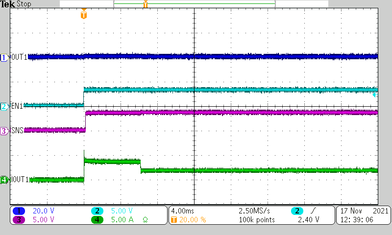 Figure 10-6 Enabling Into Short
(RILIM = 10 k, VS = 6 V, Delay = 6 mS)
Figure 10-6 Enabling Into Short
(RILIM = 10 k, VS = 6 V, Delay = 6 mS)In Figure 10-6, the output is also permanently shorted. Upon enabling the device, the current reaches the 2 times current limit, however because the power dissipation is greater due to the higher input voltage at VS the device reaches its thermal shutdown threshold and disables itself before reaching the programmed delay time.
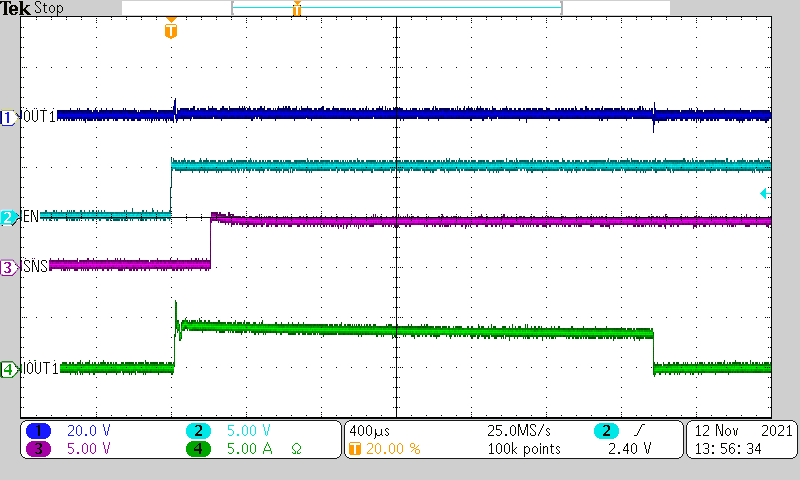 Figure 10-7 Enabling Into Short (RILIM = 10 k, VS = 24 V, Delay = 6
mS)
Figure 10-7 Enabling Into Short (RILIM = 10 k, VS = 24 V, Delay = 6
mS)Figure 10-8 shows that after the device has been enabled into a short and due to the high power dissipation, the device reaches its thermal shutdown threshold. The device then shuts down the FET for a period of tRETRY and re-enables the FET into the short. The capture shows the continuous retry cycle and protection because the short is permanently applied.
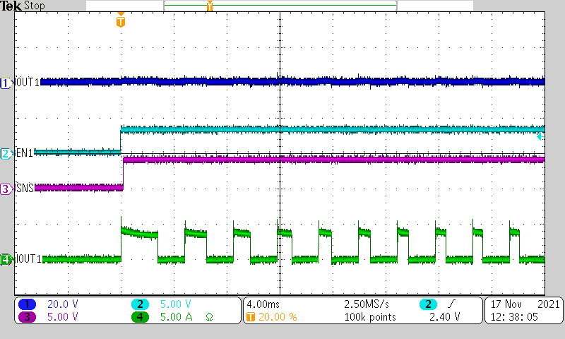 Figure 10-8 Permanent Short Behavior
(RILIM = 10 k, VS = 24 V, Delay = 6 mS)
Figure 10-8 Permanent Short Behavior
(RILIM = 10 k, VS = 24 V, Delay = 6 mS)In the event a short is applied to the output while a load is being driven, the device activates its fast trip comparator and shutdown the output to limit the inrush current. The device then immediately re-enables into the short and limit the current to the programmed current limit value. Figure 10-9 describes the behavior.
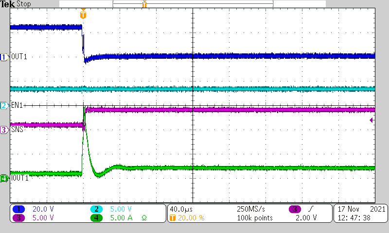 Figure 10-9 On-State Short Circuit
(RILIM = 10 k, VS = 24 V )