SLVU047A February 2001 – March 2022 TPS2330 , TPS2331 , TPS5102
4 Layouts of the EVM and the Interface Card
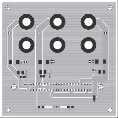
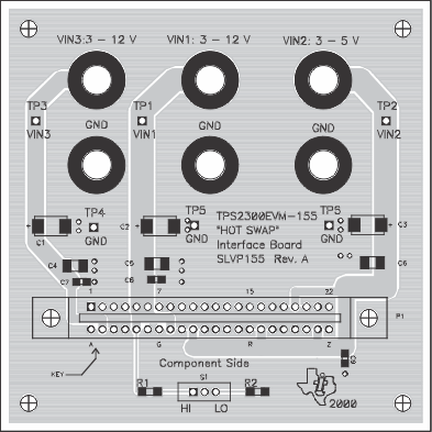
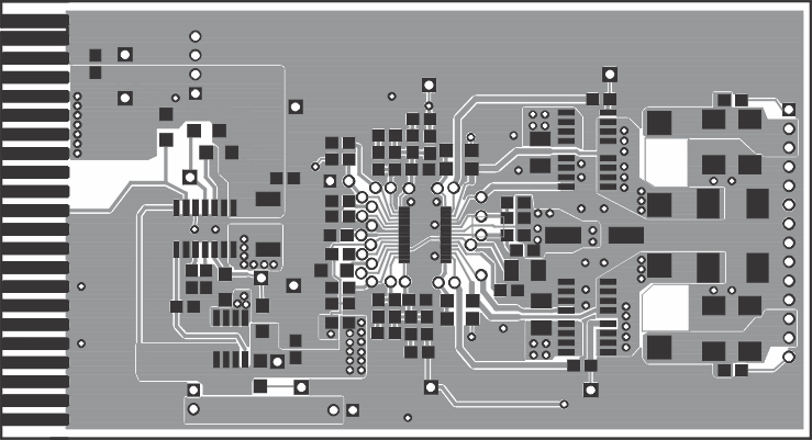
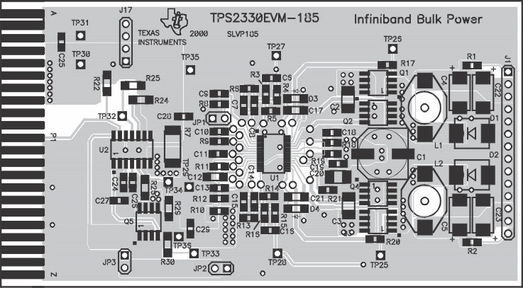
Figure 4-1 through Figure 4-4 illustrate the placements of the components and the top-layer layouts for both the InfiniBand bulk power EVM and the interface card, respectively. All the components are placed on the top layers only. The bottom layers are ground planes except for a few short traces on the InfiniBand bulk power EVM.
 Figure 4-1 Top Layer of the Interface
Card and Placement of the Components (Top Layer)
 Figure 4-2 Top Layer of the Interface
Card and Placement of the Components (Top Assembly)
 Figure 4-3 Top Layer of the InfiniBand
Bulk Power EVM and Placement of the Components (Top Layer)
 Figure 4-4 Top Layer of the InfiniBand
Bulk Power EVM and Placement of the Components (Top Assembly)