SLVU380A September   2010  – October 2021 TPS54320


  1.   Trademarks
  2. 1Introduction
    1. 1.1 Background
    2. 1.2 Performance Specification Summary
    3. 1.3 Modifications
      1. 1.3.1 Output Voltage Set Point
      2. 1.3.2 Slow Start Time
      3. 1.3.3 Track In
      4. 1.3.4 Adjustable UVLO
      5. 1.3.5 Input Voltage Rails
  3. 2Test Setup and Results
    1. 2.1  Input / Output Connections
    2. 2.2  Efficiency
    3. 2.3  Output Voltage Load Regulation
    4. 2.4  Output Voltage Line Regulation
    5. 2.5  Load Transients
    6. 2.6  Loop Characteristics
    7. 2.7  Output Voltage Ripple
    8. 2.8  Input Voltage Ripple
    9. 2.9  Powering Up
    10. 2.10 Thermal Characteristics
  4. 3Board Layout
    1. 3.1 Layout
    2. 3.2 Estimated Circuit Area
  5. 4Schematic and Bill of Materials
    1. 4.1 Schematic
    2. 4.2 Bill of Materials
  6. 5Revision History

Output Voltage Ripple

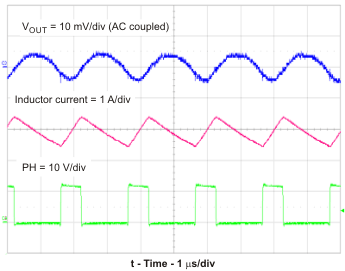
Figure 2-7 shows the TPS54320 output voltage ripple. The output current is the rated full load of 3 A and VIN = 12 V. The ripple voltage is measured directly across the output capacitors with a low inductance probe. Measuring at the output test points, TP8 and TP9, can pick up some radiated noise and give an erroneous measurement.
GUID-AA843D45-CB2E-40C5-B6E2-0C066075214E-low.gifFigure 2-7 TPS54320 Output Ripple