SLVU490A October 2011 – October 2021 TPS54295
- Trademarks
- 1Introduction
- 2Performance Specification Summary
- 3Modifications
- 4Test Setup and Results
- 5Board Layout
- 6Schematic, Bill of Materials, and Reference
- 7Revision History
3.1 Output Voltage Setpoint
To change the output voltages of the EVM, it is necessary to change the value of the top resistor of the feedback divider, R1 or R3. Please refer to the top assembly in Figure 5-1 to locate the resistors close to the output connectors. Changing the value of R1 or R3 can change the output voltage above 0.765 V. The value of R1 or R3 for a specific output voltage can be calculated using Equation 1.
For output voltage from 0.76 V to 7 V:
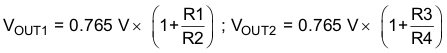
Table 3-1 lists the R1 or R3 values for some common output voltages. For output voltages of 1.8 V or above, a feedforward capacitor (C21 or C20) may be required to improve the phase margin. Pads for this component (C21 or C20) are provided on the printed-circuit board. Note that the resistor values given in Table 3-1 are standard values and not the exact values calculated using Equation 1.
| Output Voltage (V) | R1, R3 (kΩ) | R2, R4 (kΩ) | C21, C20 (pF) | L1, L2 (µH) | C14. C15, C18 Total Capacitance, C16. C17, C19 Total Capacitance (µF) |
|---|---|---|---|---|---|
| 1 | 6.81 | 22.1 | 1.0 - 1.5 | 22 - 68 | |
| 1.05 | 8.25 | 22.1 | 1.0 - 1.5 | 22 - 68 | |
| 1.2 | 12.7 | 22.1 | 1.0 - 1.5 | 22 - 68 | |
| 1.5 | 21.5 | 22.1 | 1.5 | 22 - 68 | |
| 1.8 | 30.1 | 22.1 | 5 - 22 | 1.5 | 22 - 68 |
| 2.5 | 49.9 | 22.1 | 5 - 22 | 2.2 | 22 - 68 |
| 3.3 | 73.2 | 22.1 | 5 - 22 | 2.2 | 22 - 68 |
| 5 | 124 | 22.1 | 5 - 22 | 3.3 | 22 - 68 |