SLVU493A October 2011 – October 2021 TPS54229
4.9 Start-Up
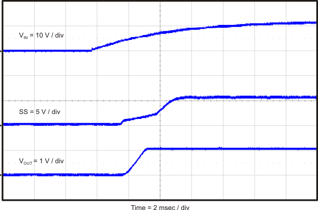
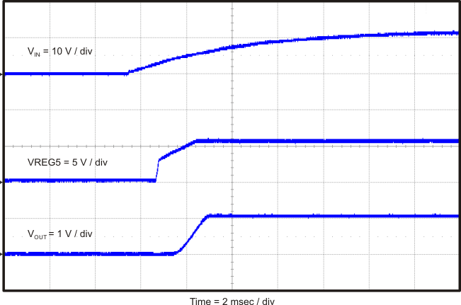
The TPS54229EVM-056 start-up waveforms relative to VIN are shown in Figure 4-8 and Figure 4-9.
 Figure 4-8 TPS54229EVM-056 Start-Up Relative to VIN With SS
 Figure 4-9 TPS54229EVM-056 Start-Up Relative to VIN With VREG5
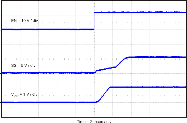
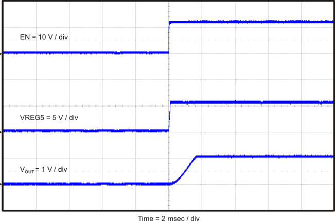
The TPS54229EVM-056 start-up waveforms relative to enable (EN) are shown in Figure 4-10 and Figure 4-11.
 Figure 4-10 TPS54229EVM-056 Start-Up Relative to EN With SS
 Figure 4-11 TPS54229EVM-056 Start-Up Relative to EN With VREG5