SLVUA15A January 2014 – August 2021 TPS562209
3.1 Output Voltage Setpoint
To change the output voltage of the EVMs, it is necessary to change the value of resistor R5. Changing the value of R5 can change the output voltage above 0.765 V. The value of R5 for a specific output voltage can be calculated using Equation 1.
Equation 1. 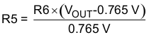
Table 3-1 lists the R5 values for some common output voltages. For higher output voltages of 1.8 V or above, a feedforward capacitor (C9) may be used to improve phase margin. Pads for this component (C9) are provided on the printed-circuit board (PCB). Note that the values given in Table 3-1 are standard values and not the exact value calculated using Table 3-1.
Table 3-1 Output Voltages
| Output Voltage (V) | R5 (kΩ) | R6 (kΩ) | C9 (pF) | L1 (µH) | C6 + C7 +C8 (µF) | ||
|---|---|---|---|---|---|---|---|
| Min | Typ | Max | |||||
| 1.0 | 15.4 | 49.9 | 1.5 | 2.2 | 4.7 | 20 - 68 | |
| 1.05 | 18.7 | 49.9 | 1.5 | 2.2 | 4.7 | 20 - 68 | |
| 1.2 | 28.7 | 49.9 | 1.5 | 2.2 | 4.7 | 20 - 68 | |
| 1.5 | 47.5 | 49.9 | 1.5 | 2.2 | 4.7 | 20 - 68 | |
| 1.8 | 68.1 | 49.9 | optional, 10 pF max | 1.5 | 2.2 | 4.7 | 20 - 68 |
| 2.5 | 113 | 49.9 | optional, 10 pF max | 2.2 | 3.3 | 4.7 | 20 - 68 |
| 3.3 | 165 | 49.9 | optional, 10 pF max | 2.2 | 3.3 | 4.7 | 20 - 68 |
| 5.0 | 274 | 49.9 | optional, 10 pF max | 3.3 | 4.7 | 4.7 | 20 - 68 |
| 6.5 | 374 | 49.9 | optional, 10 pF max | 3.3 | 4.7 | 4.7 | 20 - 68 |